14
14-6
REAL TIME DEBUGGER (RTD)
14.3 Functional Description of the RTD
32180 Group User’s Manual (Rev.1.0)
32 clock
periods
32 clock
periods
WRR(A1) (A1) Write data
3 clock periods
RTDCLK
RTDRXD
RTDTXD
RTDACK
WRR(A2) (A2) Write data
D (A1) Read value
before writing
D (A1) Verify value
after writing
Notes: • (An) = Specified address
• D
An
= Data at specified address
An
32 clock
periods
32 clock
periods
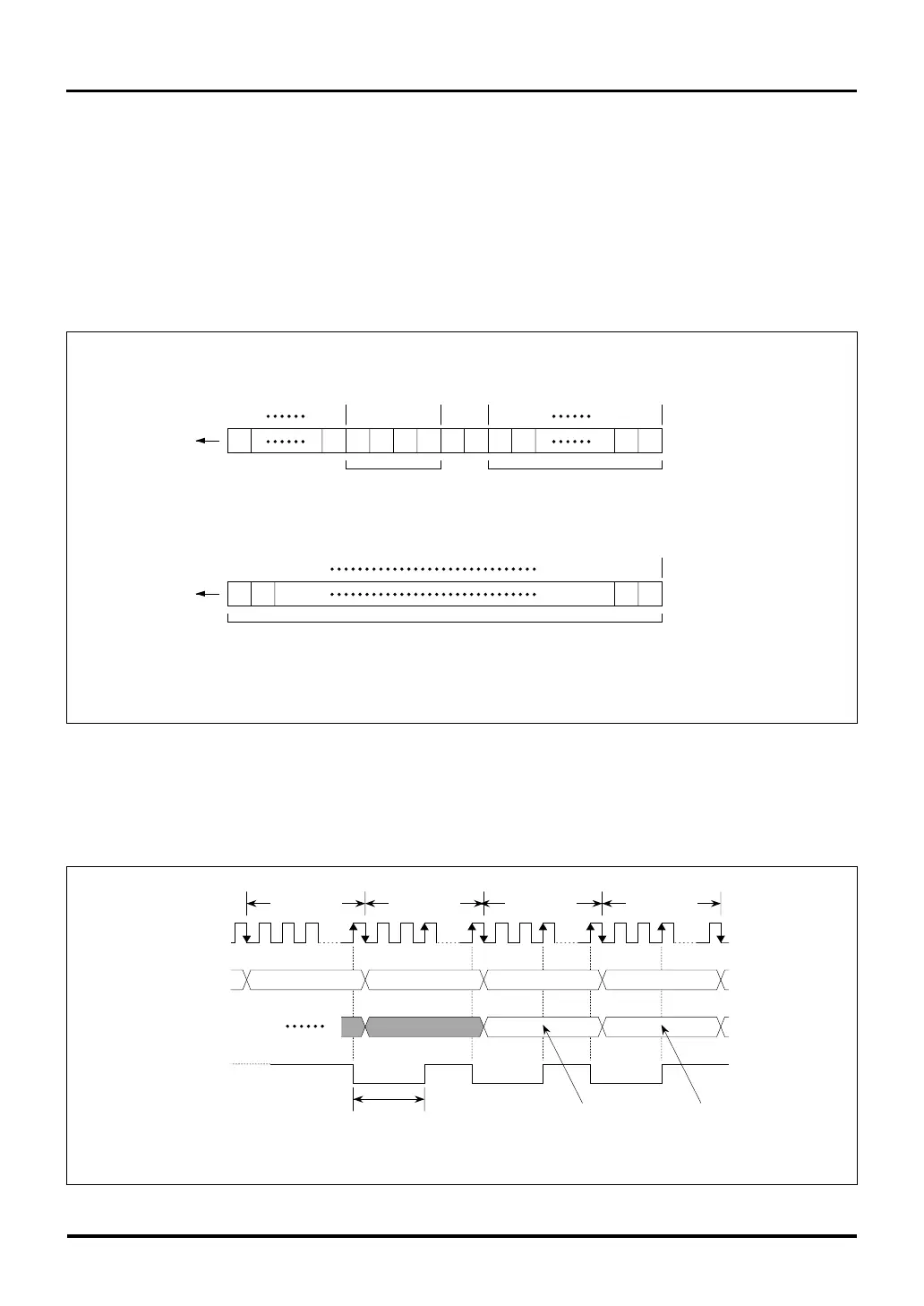
Figure 14.3.5 Operation of the WRR Command
14.3.3 Operation of the WRR (RAM Content Forcible Rewrite)
When the WRR (RAM content forcible rewrite) command is issued, the RTD forcibly rewrites the contents of the
internal RAM without causing the CPU’s internal bus to stop. Because the RTD writes data to the internal RAM
while there are no transfers performed between the CPU and internal RAM, no extra CPU load is incurred.
Only the 32-bit word-aligned addresses can be specified for read from the internal RAM. (The two low-order
address bits specified by a command are ignored.) Data are written to the internal RAM in 32-bit units.
The external host should transmit the command and address in the first frame and then the write data in the
second frame. The RTD writes to the internal RAM in the third frame after receiving the write data.
Figure 14.3.4 WRR Command Data Format
The RTD reads out data from the specified address before writing to the internal RAM and again reads out data
from the same address immediately after writing to the internal RAM (this helps to verify the data written to the
internal RAM). The read data is output at the timing shown below.
31
X 0 0 11
19 18 17
16
0
15
0
14 13 12 1
A16
0
X
20
A17A28A29
Command (WRR) Specified address
Notes: • X = Don't care. (However, if issued immediately after the RCV command, bits 20-31 must all be set to 1.)
• The specified address and write data are transferred LSB-first.
31
b31
1
b0
0
b30
30
b1
Write data
RTDRXD
(MSB side)
(MSB side)
(LSB side)
(LSB side)
RTDRXD
a) First frame
b) Second frame

 Loading...


