10
10-171
MULTIJUNCTION TIMERS
10.8 TOU (Output-Related 24-Bit Timer)
32180 Group User’s Manual (Rev.1.0)
10.8.9 PWMOFF Input Processing Control Registers
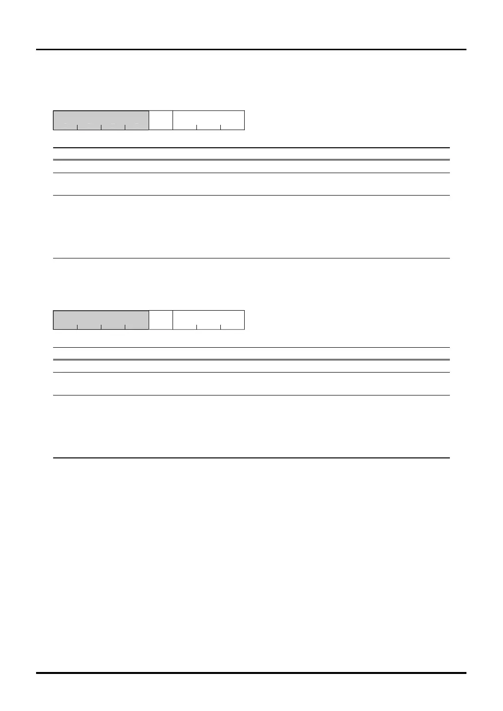
PWMOFF0 Input Processing Control Register (PWMOFF0CR) <Address: H'0080 07E0>
123456b7b0
PWMOFF0SPWM
OFF0SP
0000
<After reset: H’00>
b Bit Name Function R W
0–3 No function assigned. Fix to "0". 00
4 PWMOFF0SP 0W
PWMOFF0S write control bit
5–7 PWMOFF0S 000: Input has no effect R W
PWMOFF0 input processing control bit 001: Rising edge
010: Falling edge
011: Both edges
10X: Low level
11X: High level
PWMOFF1 Input Processing Control Register (PWMOFF1CR) <Address: H'0080 0BE0>
123456b7b0
PWMOFF1SPWM
OFF1SP
0000
<After reset: H’00>
b Bit Name Function R W
0–3 No function assigned. Fix to "0". 00
4 PWMOFF1SP 0W
PWMOFF1S write control bit
5–7 PWMOFF1S 000: Input has no effect R W
PWMOFF1 input processing control bit 001: Rising edge
010: Falling edge
011: Both edges
10X: Low level
11X: High level

 Loading...


