17
17-3
RAM BACKUP MODE
32180 Group User's Manual (Rev.1.0)
Figure 17.2.1 Typical Circuit for RAM Backup at Power Outage
VREFn
SBI#
ADnINi
M32R/ECU
(Note 2)
Backup battery
VCC VDDE
VBB
VREF
Reference voltage for
power outage detection
Power outage
detection signal
Backup power supply
for power outage
Power supply monitor IC
Note 1: Power outage is detected by the DC IN (regulator input) voltage.
Note 2: These pins are used to detect a RAM backup signal.
Note 3: This pin outputs a high when the power is on and outputs a low when the power is down.
VDDE
DC IN
Input Output
Regulator
AVCCn VCC-BUS OSC-VCC
OUT
(Note 3)
VCCE
(Note 1)
C
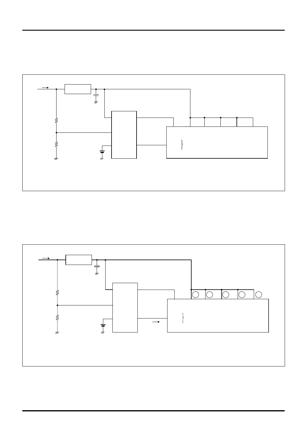
17.2 Example of RAM Backup when Power is Down
A typical circuit for RAM backup at power outage is shown in Figure 17.2.1. The following explains how the RAM
can be backed up by using this circuit as an example.
17.2.1 Normal Operating State
Figure 17.2.2 shows the normal operating state of the M32R/ECU. During normal operation, input on the SBI#
pin or ADnINi (i = 0–15) pin which is used to detect a RAM backup signal remains high.
Figure 17.2.2 Normal Operating State (when VCCE = 5 V)
VREFn
SBI#
ADnINi
M32R/ECU
(Note 2)
VCC VDDE
VBB
VREF
Note 1: Power outage is detected by the DC IN (regulator input) voltage.
Note 2: These pins are used to detect a RAM backup signal.
Note 3: This pin outputs a high when the power is on and outputs a low when the power is down.
VDDE
DC IN
Regulator
AVCCn VCC-BUS OSC-VCC
OUT
(Note 3)
(Note 4)
VCCE
C
"H"
5V5V5V5V5V
Input
Output
Reference voltage for
power outage detection
(Note 1)
Backup battery
Power supply monitor IC
Backup power supply
for power outage
Power outage
detection signal
Note 4: Backup power supply = 3.0 to 5.5 V
17.2 Example of RAM Backup when Power is Down

 Loading...


