21
21-27
ELECTRICAL CHARACTERISTICS
32180 Group User's Manual (Rev.1.0)
21.7.3 A.C. Characteristics
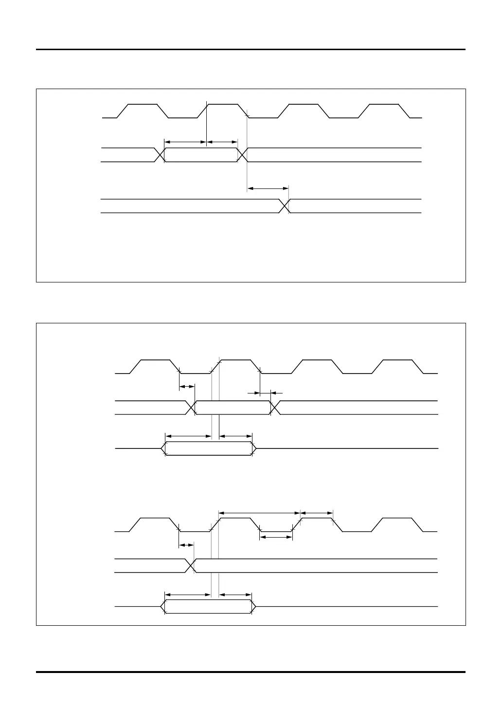
Figure 21.7.1 Input/Output Port Timing
Figure 21.7.2 Serial I/O Timing
Port output
[3]
td(E-P)
0.8VCCE
0.2VCCE
BCLK
0.8VCCE
0.2VCCE
0.8VCCE
0.2VCCE
Port input
0.2VCCE
0.8VCCE
[1]
tsu(P-E)
[2]
th(E-P)
Note: • The ports listed below operate with the VCC-BUS power supply, and not with the VCCE power supply.
Therefore, the reference voltage for these ports is the VCC-BUS input voltage.
P00–P07, P10–P17, P20–P27, P30–P37, P41–P47, P70–P73, P224, P225
SCLKO
TXD
RXD
[6]
td(CLK-D)
[4] tsu(D-CLK) [5] th(CLK-D)
a)
CSIO mode, with internal clock selected
0.8VCCE
0.2VCCE
0.2VCCE
0.8VCCE
0.2VCCE
0.8VCCE
b)
CSIO mode, with external clock selected
SCLKI
TXD
RXD
[12]
td(CLK-D)
[10] tsu(D-CLK) [11] th(CLK-D)
0.8VCCE
0.2VCCE
0.2VCCE
0.8VCCE
0.2VCCE
0.8VCCE
0.2VCCE
0.8VCCE
[7] tc(CLK) [8] tw(CLKH)
[9] tw(CLKL)
0.2VCCE
0.8VCCE
[98] th(CLK-D)
21.7 A.C. Characteristics (when VCCE = 5 V)

 Loading...


