21
21-26
ELECTRICAL CHARACTERISTICS
32180 Group User's Manual (Rev.1.0)
Symbol Parameter Rated Value Unit See Figs.
21.7.8
MIN MAX
21.7.9
21.7.10
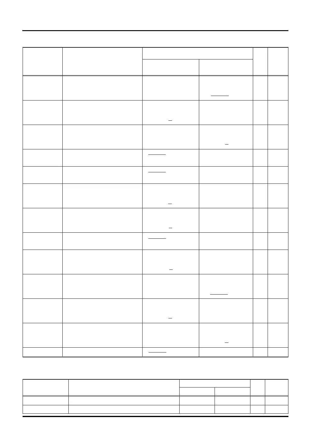
td(BLWL-D) Data Output Delay Time after Write With zero wait state: 5 ns [52]
td(BHWL-D) (byte write mode) With 1 or more wait states:
15-( )×S
tv(BLWH-D) Data Output Valid Time after Write With zero wait state: -7 ns [53]
tv(BHWH-D) (byte write mode) With 1 or more wait states:
tc(BCLK)×( +R)-13
tpxz(BLWH-DZ) Data Output Disable Time after Write With zero wait state: 5 ns [54]
tpxz(BHWH-DZ) (byte write mode) With 1 or more wait states:
tc(BCLK)×( +R)+5
td(A-WRL) Address Delay Time before Write ( )×(1+S)-15 ns [69]
(byte enable mode)
td(CS-WRL) Chip Select Delay Time before Write ( )×(1+S)-15 ns [70]
(byte enable mode)
tv(WRH-A) Address Valid Time after Write With zero wait state: -5 ns [71]
(byte enable mode) With 1 or more wait states:
tc(BCLK)×( +R)-5
tv(WRH-CS) Chip Select Valid Time after Write With zero wait state: -5 ns [72]
(byte enable mode) With 1 or more wait states:
tc(BCLK)×( +R)-5
td(BLE-WRL) Byte Enable Delay Time before Write ( )×(1+S)-15 ns [73]
td(BHE-WRL) (byte enable mode)
tv(WRH-BLE) Byte Enable Valid Time after Write With zero wait state: -5 ns [74]
tv(WRH-BHE) (byte enable mode) With 1 or more wait states:
tc(BCLK)×( +R)-5
td(WRL-D) Data Output Delay Time after Write With zero wait state: 7 ns [75]
(byte enable mode) With 1 or more wait states:
15-( )×S
tv(WRH-D) Data Output Valid Time after Write With zero wait state: -7 ns [76]
(byte enable mode) With 1 or more wait states:
tc(BCLK)×( +R)-13
tpxz(WRH-DZ) Data Output Disable Time after Write With zero wait state: 5 ns [77]
(byte enable mode) With 1 or more wait states:
tc(BCLK)×( +R)+5
tw(RDH) Read High Pulse Width ( )×(1+S)-5 ns [55]
Read and write timing (continued from the preceding page)
(5) Bus arbitration
Symbol Parameter Rated Value Unit See Fig.
MIN MAX 21.7.11
td(BCLKL-HACKL) HACK# Delay Time after BCLK 29 ns [37]
tv(BCLKL-HACKL) HACK# Valid Time after BCLK -11 ns [38]
tc(BCLK)
2
1
2
tc(BCLK)
2
tc(BCLK)
2
1
2
1
2
tc(BCLK)
2
1
2
tc(BCLK)
2
1
2
1
2
tc(BCLK)
2
1
2
21.7 A.C. Characteristics (when VCCE = 5 V)

 Loading...


