21
21-13
ELECTRICAL CHARACTERISTICS
32180 Group User's Manual (Rev.1.0)
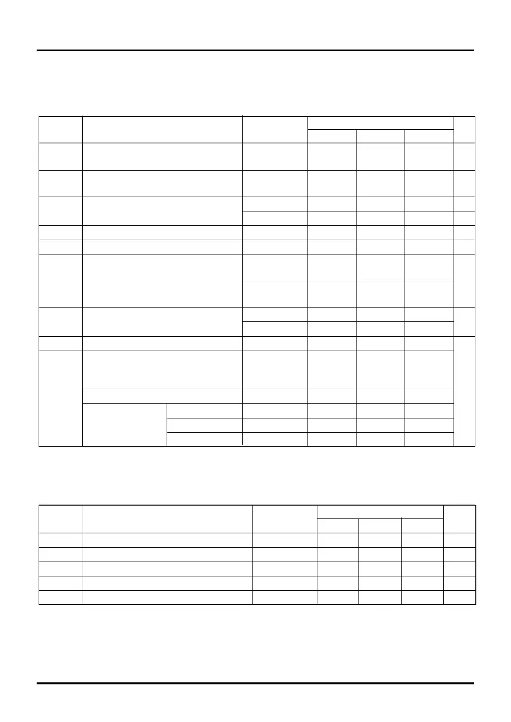
Symbol Parameter Test Condition Rated Value Unit
MIN TYP MAX
ICCE VCCE/OSC-VCC Power Supply Current When Operating f(XIN)=10.0MHz 120 mA
IDDE VDDE Power Supply Current When Operating f(XIN)=10.0MHz 1 mA
ICC-BUS VCC-BUS Power Supply Current When Operating f(XIN)=10.0MHz 7 mA
IAVCC AVCC Power Supply Current When Operating f(XIN)=10.0MHz 2 mA
IVREF VREF Power Supply Current When Operating f(XIN)=10.0MHz 1 mA
Symbol Parameter Test Condition Rated Value Unit
MIN TYP MAX
VOH Output High Voltage IOH≥-2mA VCCE+0.5 VCCE V
×
IOH(mA)
VOL Output Low Voltage IOL≤2mA 0 0.225
×
IOL V
(mA)
VDDE RAM Retention Power Supply Voltage When operating 3.0 3.6 V
During backup 3.0 3.6 V
IIH High State Input Current VI=VCCE -5 5 µA
IIL Low State Input Current VI=0V -5 5 µA
ICC Total Power Supply Current (Note 1) f(XIN)=10.0MHz, 75 mA
When reset
f(XIN)=10.0MHz, 80 120
When operating
IDDEhold RAM Retention Power Supply Current Ta=25C° 0.5 10 µA
Ta=85C° 300
VT+- FP, MOD0, 1, JTMS, JTRST, JTDI, RESET 0.65 V
VT- Standard input for the following pins: 0.5
RTDCLK, RTDRXD, SCLKI0, 1, 4, 5, RXD0–5,
TCLK0–3, TIN0–33, CRX0, 1
Standard input for the following pins: SBI, HREQ 0.2
When threshold 0.7VCCE/0.35VCCE 0.5
switching function 0.7VCCE/0.5VCCE 0.2
is used (VT+ / VT–) 0.5VCCE/0.35VCCE 0.2
Note 1: Total amount of current when VCCE = OSC-VCC = VCC-BUS = VDDE = AVCC = VREF in single-chip mode
21.4.2 D.C. Characteristics (when VCCE = 3.3 V ± 0.3 V, f(XIN) = 10 MHz)
Electrical Characteristics (Referenced to VCCE, OSC-VCC, VCC-BUS, VDDE = 3.3 V ± 0.3 V, Ta = –40°C to
85°C Unless Otherwise Noted)
Electrical Characteristics of Each Power Supply Pin
21.4 Electrical Characteristics when VCCE = 3.3 V, f(XIN) = 10 MHz

 Loading...


