21
21-36
ELECTRICAL CHARACTERISTICS
32180 Group User's Manual (Rev.1.0)
(3) SBI
21.8 A.C. Characteristics (when VCCE = 3.3 V)
• The timing conditions are referenced to VCCE, OSC-VCC, VCC-BUS, VDDE = 3.3V ± 0.3 V, Ta = –40°C to
125°C unless otherwise noted.
• The rated values below are guaranteed for the case where the output load capacitance of the measured pins
are 15 pF to 50 pF (for JTAG related values, a concentrated capacitance of 80 pF).
• The terms S, R, ID and W in the rated values shown below have the following meaning:
S: "1" when the CS Area Wait Control Register SWAIT bit = 1, or "0" when SWAIT bit = 0
R: "1" when the CS Area Wait Control Register RECOV bit = 1, or "0" when RECOV bit = 0
ID: Number of idle cycles inserted at the end of the bus cycle. Idle cycles may be inserted as specified by the
CS Area Wait Control Register IDLE bit, or inserted by default when a write operation is executed immediately
after a read (ID = 0 or 1).
W: Number of wait states (selected by the WTCSEL bit)
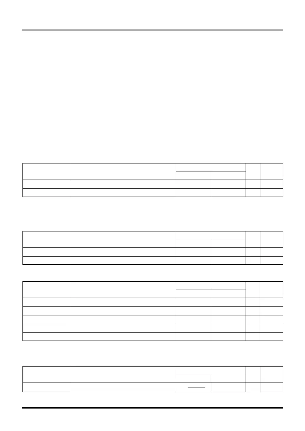
21.8.1 Timing Requirements
(1) Input/output ports
Symbol Parameter Rated Value Unit See Fig.
MIN MAX 21.8.1
tsu(P-E) Port Input Setup Time 100 ns [1]
th(E-P) Port Input Hold Time 0 ns [2]
(2) Serial I/O
a) CSIO mode, with internal clock selected
Symbol Parameter Rated Value Unit See Fig.
MIN MAX 21.8.2
tsu(D-CLK) RXD Input Setup Time 150 ns [4]
th(CLK-D) RXD Input Hold Time 50 ns [5]
b) CSIO mode, with external clock selected
Symbol Parameter Rated Value Unit See Fig.
MIN MAX 21.8.2
tc(CLK) CLK Input Cycle Time 640 ns [7]
tw(CLKH) CLK Input High Pulse Width 300 ns [8]
tw(CLKL) CLK Input Low Pulse Width 300 ns [9]
tsu(D-CLK) RXD Input Setup Time 60 ns [10]
th(CLK-D) RXD Input Hold Time 100 ns [11]
Symbol Parameter Rated Value Unit See Fig.
MIN MAX 21.8.3
tw(SBIL) SBI# Input Pulse Width 5
×
ns [13]
tc(BCLK)
2
21.8 A.C. Characteristics (when VCCE = 3.3 V)

 Loading...


