15
15-9
EXTERNAL BUS INTERFACE
32180 Group User’s Manual (Rev.1.0)
15.2.3 Bus Mode Control Register
Bus Mode Control Register (BUSMODC) <Address: H’0080 077F>
9 1011121314b15b8
BUSMOD
0
<After reset: H’00>
b Bit Name Function R W
8–14 No function assigned. Fix to "0". 00
15 BUSMOD 0: WR signal separate mode R W
Bus mode control bit 1: Byte enable separate mode
This register is used to facilitate memory connections during processor mode and external extension mode.
When the Bus Mode Control bit (BUSMOD) = "0", the WR# signal is output separately for each byte area.
Signals RD#, BHW#, BLW#, BCLK# and WAIT# can be used.
When the Bus Mode Control bit (BUSMOD) = "1", the byte enable signal is output separately for each byte area.
Signals RD#, BHE#, BLE#, WR# and WAIT# can be used. In a WAIT control circuit configuration, because
BCLK output is not available, timing must be controlled external to the chip.
Note: • Any external bus area must temporarily be accessed for read or write before the Bus Mode
Control bit (BUSMOD) can be set to "1" (= byte enable separate mode).
For memory connection in boot mode, the Bus Mode Control Register has no effect, and the microcomputer
operates in the same way as when the Bus Mode Control bit (BUSMOD) is cleared to "0".
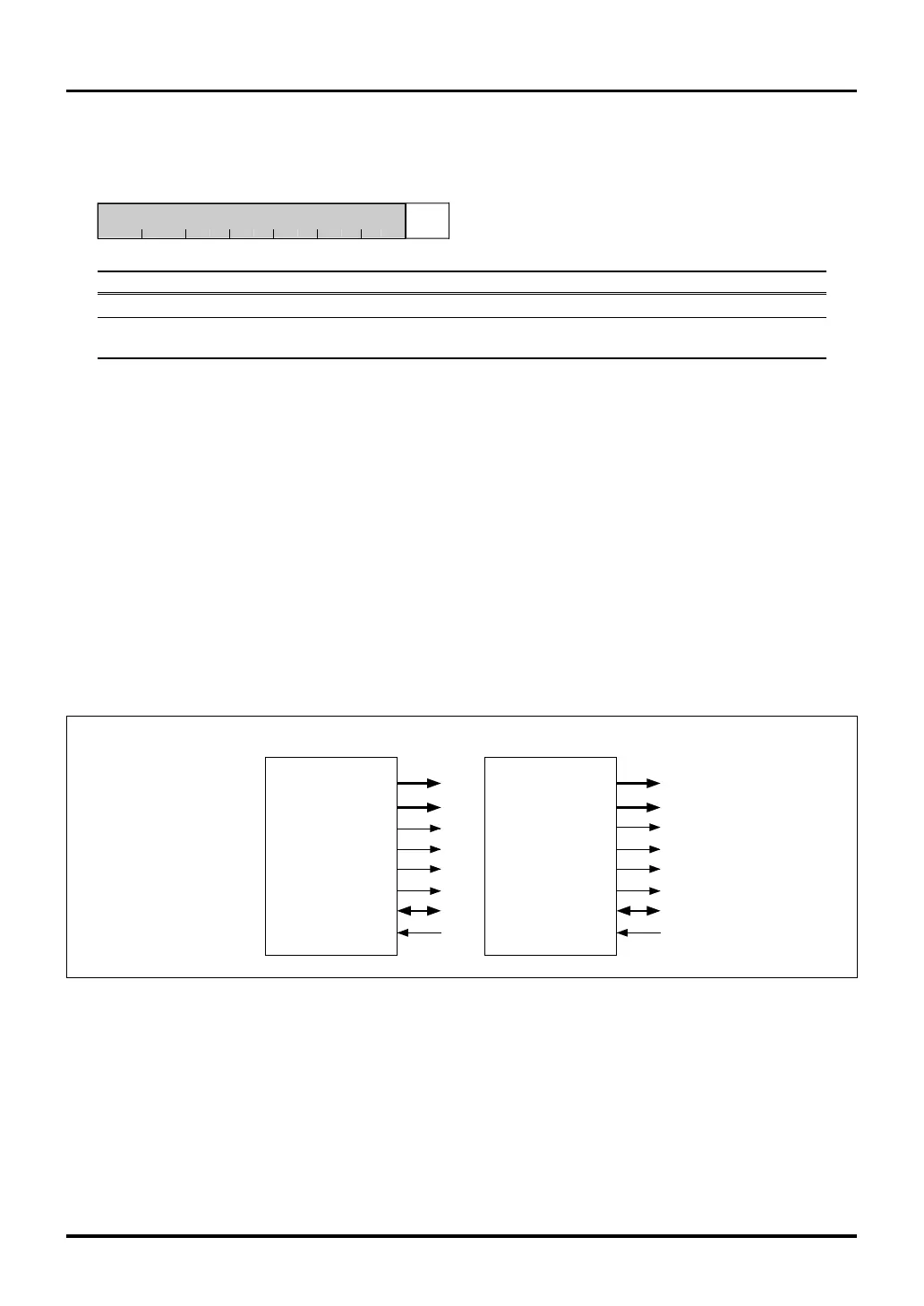
Figure 15.2.1 Pin Functions when External Bus Modes are Changed
CS0#–CS3#
DB0–DB15
WAIT#
RD#
BHW#
BLW#
A11–A30
CS0#–CS3#
DB0–DB15
WAIT#
RD#
WR#
BHE#
BLE#
A11–A30
BCLK
BUSMOD bit = 0 BUSMOD bit = 1
15.2 External Bus Interface Related Registers

 Loading...


