1
1-5
OVERVIEW
32180 Group User’s Manual (Rev.1.0)
1.2 Block Diagram
1.2 Block Diagram
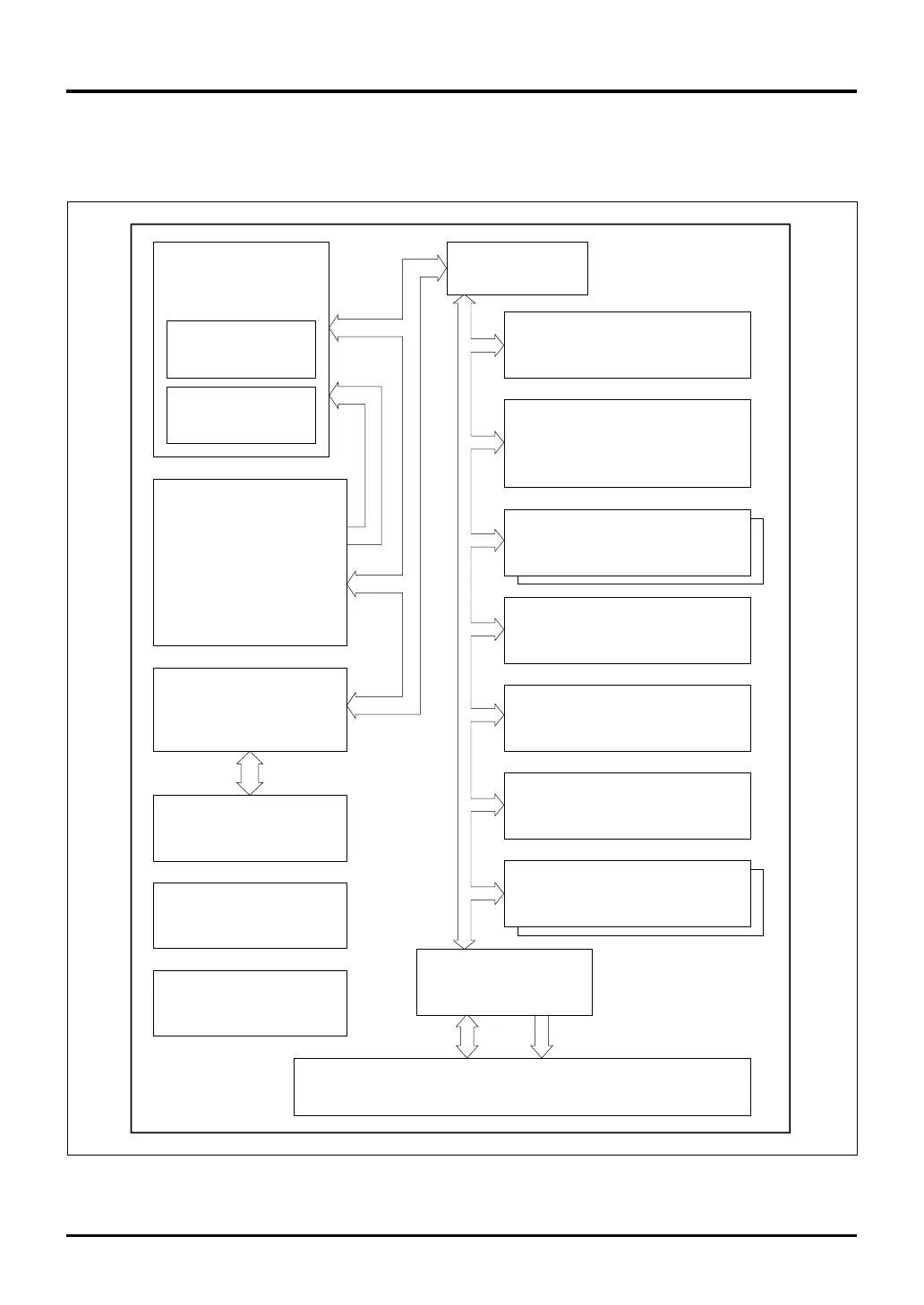
Figure 1.2.1 shows a block diagram of the 32180. The features of each block are described in Table 1.2.1.
Figure 1.2.1 Block Diagram of the 32180
PLL Clock Generator
Internal Bus
Interface
AddressData
Internal RAM
(48 Kbytes)
Internal Flash Memory
(1 Mbytes = 1,024 Kbytes)
M32R-FPU Core
(80 MHz)
Multiplier/Accumulator
(32 bits × 16 bits + 56 bits)
DMAC
(10 channels)
Multijunction Timer
(64 channels)
Serial I/O
(6 channels)
A-D Converter × 2
(A-D0 : 10-bit converter, 16 channels)
(A-D1 : 10-bit converter, 16 channels)
Wait Controller
Interrupt Controller
(32 sources, 8 levels)
Real-Time Debugger
(RTD)
External Bus
Interface
Internal 32-bit bus
Input/output ports, 158 lines
Full CAN
(2 channels)
Single-precision FPU
(fully IEEE 754 compliant)
Internal 16-bit bus
Internal 32-bit bus
Internal Power Supply
Generator (VDC)

 Loading...


