21
21-12
ELECTRICAL CHARACTERISTICS
32180 Group User's Manual (Rev.1.0)
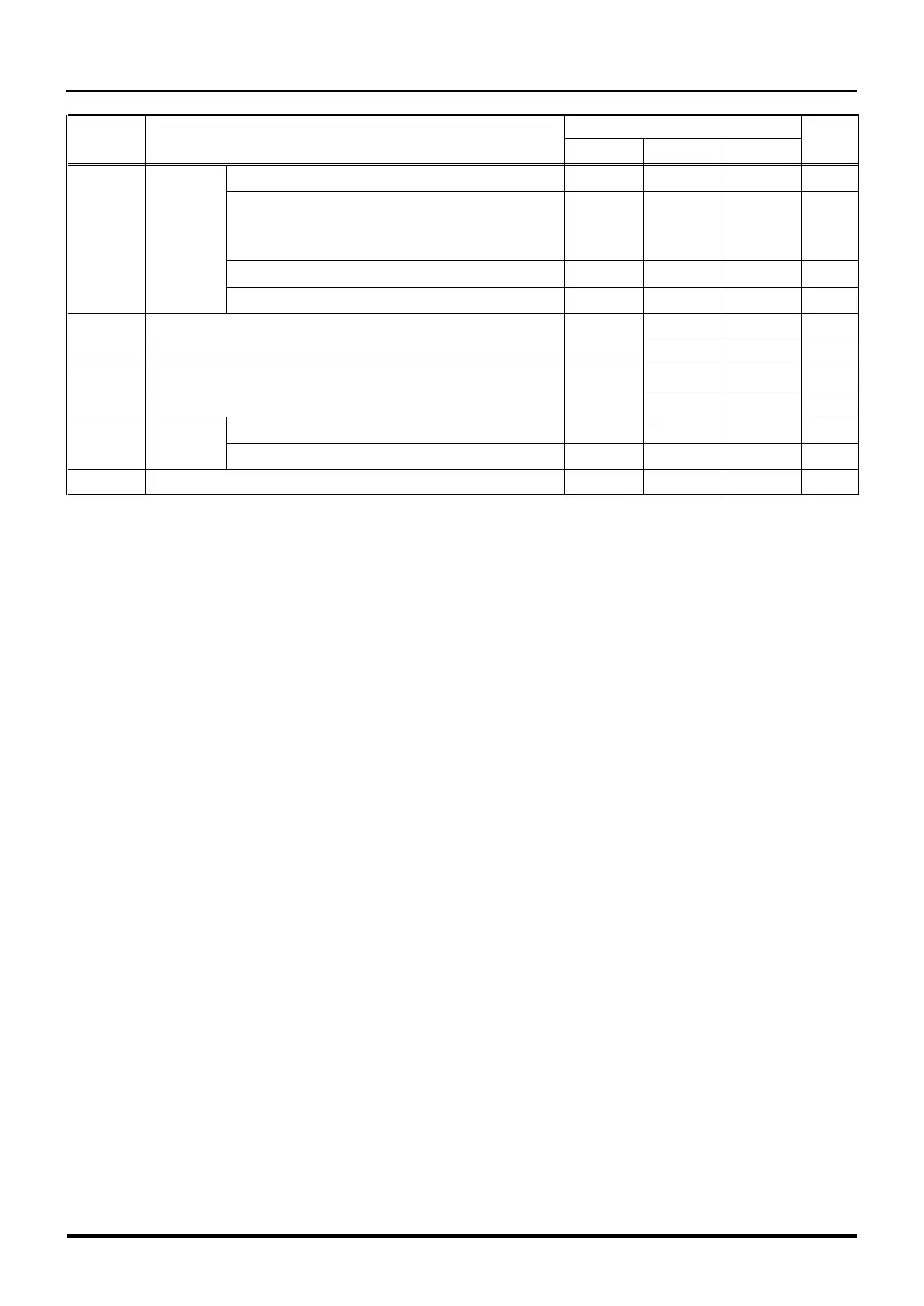
Symbol Parameter Rated Value Unit
MIN TYP MAX
VIL Input Low FP, MOD0, 1, JTMS, JTRST, JTDI, RESET 0 0.2VCCE V
Voltage
Standard input for the following pins: 0 0.2VCCE V
(Note 4) RTDCLK, RTDRXD, SCLKI0, 1, 4, 5, RXD0–5,
TCLK0–3, TIN0–33, CRX0, 1
Standard input for the following pins: DB0–15, WAIT 0 0.2VCCE V
Standard input for the followingpins: SBI, HREQ 0 0.2VCCE V
IOH(peak) High State Peak Output Current P0–P22 (Note 2) -10 mA
IOH(avg) High State Average Output Current P0–P22 (Note 3) -5 mA
IOL(peak) Low State Peak Output Current P0–P22 (Note 2) 10 mA
IOL(avg) Low State Average Output Current P0–P22 (Note 3) 5 mA
CL Output Load JTDO, JTMS 80 pF
Capacitance Other than above 50 pF
f(XIN) External Clock Input Frequency 5 10 MHz
Note 1: Subject to conditions VCCE ≥ AVCC ≥VREF, VCCE = OSC-VCC
Note 2: Make sure the total output current (peak) of ports is
| ports P0 + P1 | ≤ 80 mA
| ports P2 + P3 | ≤ 80 mA
| ports P41–P43 + P70–P73 | ≤ 80 mA
| ports P44–P47 + P224–P227 | ≤ 80 mA
| ports P61–P63 + P12 + P14 + P19 | ≤ 80 mA
| ports P65–P67 + P8 + P16 + P17 + P21 | ≤ 80 mA
| ports P74–P77 + P10 + P18 | ≤ 80 mA
| ports P9 + P11 | ≤ 80 mA
| ports P13 + P220–P223 | ≤ 80 mA
| ports P15 + P20 | ≤ 80 mA
Note 3: The average output current is a value averaged during a 100 ms period.
Note 4: The ports listed below operate with the VCC-BUS power supply, and not with the VCCE power supply. Therefore, the
reference voltage for these ports is the VCC-BUS input voltage.
P00–P07, P10–P17, P20–P27, P30–P37, P41–P47, P70–P73, P224–P227
21.4 Electrical Characteristics when VCCE = 3.3 V, f(XIN) = 10 MHz

 Loading...


