21
21-25
ELECTRICAL CHARACTERISTICS
32180 Group User's Manual (Rev.1.0)
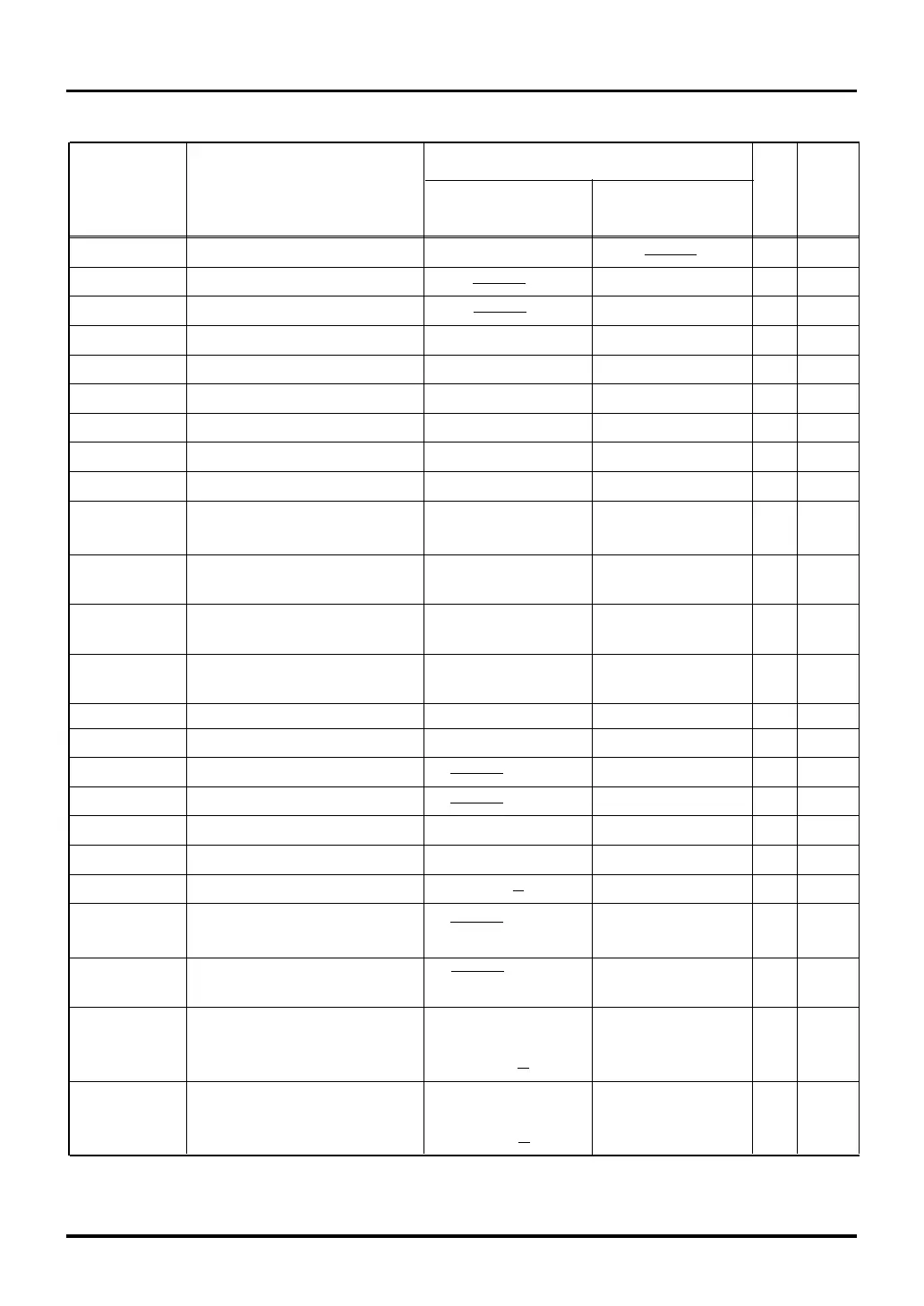
Symbol Parameter Rated Value Unit See Figs.
21.7.6
21.7.7
MIN MAX
21.7.8
21.7.9
tc(BCLK) BCLK Output Cycle Time ns [16]
tw(BCLKH) BCLK Output High Pulse Width -5 ns [17]
tw(BCLKL) BCLK Output Low Pulse Width -5 ns [18]
td(BCLKH-A) Address Delay Time after BCLK 24 ns [19]
td(BCLKH-CS) Chip Select Delay Time after BCLK 24 ns [20]
tv(BCLKH-A) Address Valid Time after BCLK -5 ns [21]
tv(BCLKH-CS) Chip Select Valid Time after BCLK -5 ns [22]
td(BCLKL-RDL) Read Delay Time after BCLK 10 ns [23]
tv(BCLKH-RDL) Read Valid Time after BCLK -5 ns [24]
td(BCLKL-BLWL) Write Delay Time after BCLK 11 ns [25]
td(BCLKL-BHWL)
tv(BCLKL-BLWL) Write Valid Time after BCLK -5 ns [26]
tv(BCLKL-BHWL)
td(BCLKL-D) Data Output Delay Time after BCLK
With zero wait state: 11 ns [27]
With 1 or more wait states: 18
tv(BCLKH-D) Data Output Valid Time after BCLK With zero wait state: -4 ns [28]
With 1 or more wait states: -10
tpzx(BCLKL-DZ) Data Output Enable Time after BCLK -10 ns [29]
tpxz(BCLKH-DZ) Data Output Disable Time after BCLK 5 ns [30]
td(A-RDL) Address Delay Time before Read ( )×(1+S)-15 ns [39]
td(CS-RDL) Chip Select Delay Time before Read ( )×(1+S)-15 ns [40]
tv(RDH-A) Address Valid Time after Read tc(BCLK)×(R+ID) ns [41]
tv(RDH-CS) Chip Select Valid Time after Read tc(BCLK)×R ns [42]
tpzx(RDH-DZ) Data Output Enable Time after Read tc(BCLK)×( +R+ID) ns [46]
td(A-BLWL) Address Delay Time before Write ( )×(1+S)-15 ns [47]
td(A-BHWL) (byte write mode)
td(CS-BLWL) Chip Select Delay Time before Write ( )×(1+S)-15 ns [48]
td(CS-BHWL) (byte write mode)
tv(BLWH-A) Address Valid Time after Write
With zero wait state: -5 ns [49]
tv(BHWH-A) (byte write mode)
With 1 or more wait states:
tc(BCLK)×( +R)-5
tv(BLWH-CS) Chip Select Valid Time after Write
With zero wait state: -5 ns [50]
tv(BHWH-CS) (byte write mode)
With 1 or more wait states:
tc(BCLK)×( +R)-5
(4) Read and write timing
tc(BCLK)
2
tc(BCLK)
2
tc(BCLK)
2
tc(BCLK)
2
tc(Xin)
2
1
2
1
2
1
2
tc(BCLK)
2
tc(BCLK)
2
21.7 A.C. Characteristics (when VCCE = 5 V)

 Loading...


