10
10-172
MULTIJUNCTION TIMERS
10.8 TOU (Output-Related 24-Bit Timer)
32180 Group User’s Manual (Rev.1.0)
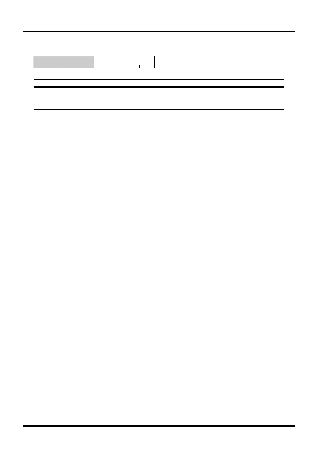
PWMOFF2 Input Processing Control Register (PWMOFF2CR) <Address: H'0080 0CE0>
123456b7b0
PWMOFF2SPWM
OFF2SP
0000
<After reset: H’00>
b Bit Name Function R W
0–3 No function assigned. Fix to "0". 00
4 PWMOFF2SP 0W
PWMOFF2S write control bit
5–7 PWMOFF2S 000: Input has no effect R W
PWMOFF2 input processing control bit 001: Rising edge
010: Falling edge
011: Both edges
10X: Low level
11X: High level
The PWMOFF input processing control registers are used to set the active edge or level entered for PWM output
disable control from an external pin. For details about the PWM output disable function, see Section 10.8.18,
“PWM Output Disable Function.”
To set the PWMOFF input processing control bits, follow the procedure described below.
1. Write data ‘1’ to the PWMOFFnS write control bit (PWMOFFnSP).
2. After 1 above, write data ‘0’ to the PWMOFFnS write control bit (PWMOFFnSP) and the set value to the
PWMOFF input processing control bits (PWMOFFnS).
Note: • If a write cycle to any other area occurs between 1 and 2, what has successively been set above
has no effect and the written value is not reflected. Therefore, disable interrupts and DMA transfers
before setting the PWMOFF control bits. Be aware that a pair of two consecutive writes comprise
a write operation.

 Loading...


