10
10-198
MULTIJUNCTION TIMERS
10.8 TOU (Output-Related 24-Bit Timer)
32180 Group User’s Manual (Rev.1.0)
F/F
F/F
F/F
F/FF/F
TIN33S
PWMOFF2S
RD
b7
P210/TO37
P211/TO38
P212/TO39
P213/TO40
P214/TO41
P215/TO42
P216/TO43
P217/TO44
P210 (internal)
P210 (internal)
P211 (internal)
P212 (internal)
P213 (internal)
P214 (internal)
P215 (internal)
P216 (internal)
P217 (internal)
P211 (internal)
P212 (internal)
P213 (internal)
P214 (internal)
P215 (internal)
IRQ18
TML1 (Cap0)
SET
b7
WR
Address
b6
PO2DISCR (WR)
PO2LVSEL
PO2LVSEL
PO2DIS
P197/TIN33/PWMOFF2
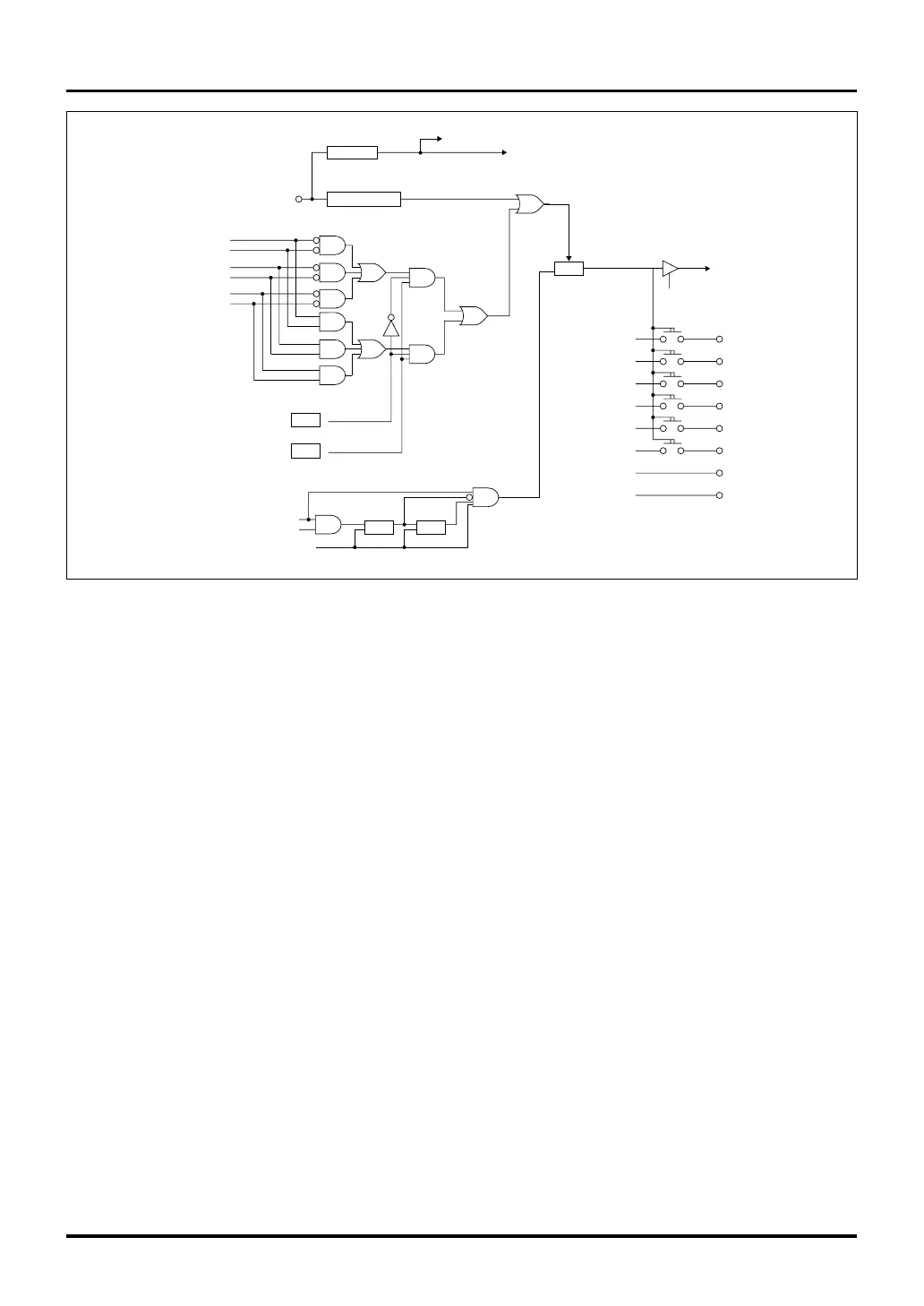
Figure 10.8.22 Circuit Configurations of the PWM Output Disable Function (2)
There are following three methods to disable PWM outputs.
(1) Using the signal entered from an external pin (TIN16/PWMOFF0, TIN17/PWMOFF1 or TIN33/PWMOFF2)
to disable PWM outputs
The input signal on the external pin (TIN16/PWMOFF0) may be used to disable outputs from the ports P160/
TO21–P165/TO26 that are provided for the PWM outputs of the TOU0_0–TOU0_5 timers. Similarly, the
input signal on the external pin (TIN17/PWMOFF1) may be used to disable outputs from the ports P180/
TO29–P185/TO34 that are provided for the PWM outputs of the TOU1_0–TOU1_5 timers. Also, the input
signal on the external pin (TIN33/PWMOFF2) may be used to disable outputs from the ports P210/TO37–
P215/TO42 that are provided for the PWM outputs of the TOU2_0–TOU2_5 timers.
To disable PWM outputs using the input signal on the external pin (TIN16/PWMOFF0, TIN17/PWMOFF1 or
TIN33/PWMOFF2), set up the PWMOFF Input Processing Control Register (PWMOFFnCR) as described
below.
[Setting up the PWMOFF Input Processing Control Register]
When using TIN16/PWMOFF0 to disable PWM outputs
1. Write data ‘1’ to the PWMOFF0CR register PWMOFF0SP bit.
2. After 1 above, write data ‘0’ to the PWMOFF0SP bit and then data ‘000,’ ‘001,’ ‘010,’ ‘011,’ ‘10X’ or
‘11X’ to the PWMOFF0S bit in succession.
Note: • If a write cycle to any other area occurs between 1 and 2, the value written to the PWMOFF0S
bit has no effect.

 Loading...


