3
3-4
ADDRESS SPACE
32180 Group User’s Manual (Rev.1.0)
3.2 Operation Modes
The microcomputer is placed in one of the following modes depending on how CPU operation mode is set by
MOD0 and MOD1 pins. The operation mode used for rewriting the internal flash memory is described separately
in Section 6.5, “Programming the Internal Flash Memory.”
Table 3.2.1 Operation Mode Settings
MOD0 MOD1 Operation mode (Note 2)
VSS VSS Single-chip mode
VSS VCCE External extension mode
VCCE VSS Processor mode (FP = VSS)
VCCE VCCE Reserved (use inhibited)
Note 1: Connect VCCE and VSS to the VCCE input power supply and ground, respectively.
Note 2: For the operation mode used to rewrite the internal flash memory (FP = VCCE) which is not shown in the above
table, see Section 6.5, “Programming the Internal Flash Memory.”
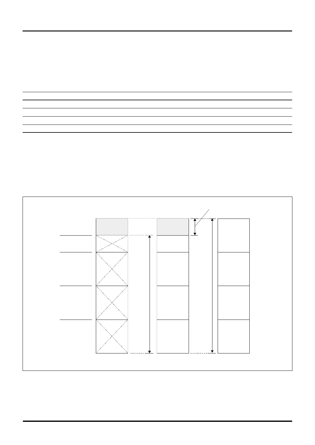
The internal ROM and extended external areas are located differently depending on how operation mode is set.
(All other areas in the address space are located the same way.) The diagram below shows how the internal ROM
and extended external areas are mapped into the address space in each operation mode. (For flash rewrite mode,
see Section 6.5, “Programming the Internal Flash Memory.”)
3.2 Operation Modes
Figure 3.2.1 Internal ROM and Extended External Area Address Mapping of the M32180F8 in Each Operation Mode
CS0 area
CS0 area
CS1 area
CS2 area
CS3 area
CS1 area
CS2 area
CS3 area
<Single-chip mode>
<External extension mode>
<Processor mode>
Non-CS0 area
Extended external area
Extended external area
H'0000 0000
H'000F FFFF
H'0010 0000
H'001F FFFF
H'0020 0000
H'003F FFFF
H'0040 0000
H'005F FFFF
H'007F FFFF
H'0060 0000
Int
rna
R
M area
(1 Mb
tes
Int
rna
R
M area
(1 Mb
tes

 Loading...


