21
21-21
ELECTRICAL CHARACTERISTICS
32180 Group User's Manual (Rev.1.0)
Symbol Parameter Rated Value Unit See Figs.
21.7.6
21.7.7
21.7.8
MIN MAX
21.7.9
21.7.10
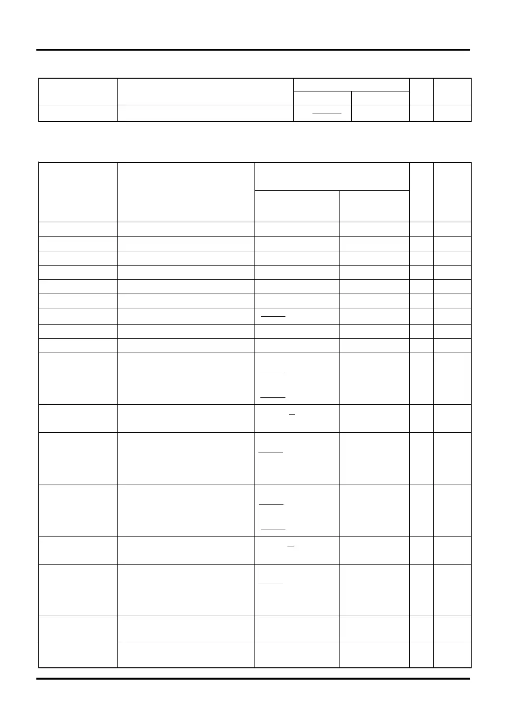
tsu(D-BCLKH) Data Input Setup Time before BCLK 26 ns [31]
th(BCLKH-D) Data Input Hold Time after BCLK 0 ns [32]
tsu(WAITL-BCLKH) WAIT# Input Setup Time before BCLK 26 ns [33]
th(BCLKH-WAITL) WAIT# Input Hold Time after BCLK 0 ns [34]
tsu(WAITH-BCLKH) WAIT# Input Setup Time before BCLK 26 ns [78]
th(BCLKH-WAITH) WAIT# Input Hold Time after BCLK 0 ns [79]
tw(RDL) Read Low Pulse Width
( )
×
(1+2W-S)-20
ns [43]
tsu(D-RDH) Data Input Setup Time before Read 30 ns [44]
th(RDH-D) Data Input Hold Time after Read 0 ns [45]
tw(BLWL) Write Low Pulse Width
With zero wait state ns [51]
tw(BHWL) (byte write mode)
-8
With 1 or more wait states
( )
×
(2W-S)-20
td(RDH-BLWL) Write Delay Time after Read tc(BCLK)
×
( +R+ID)-10 ns [56]
td(RDH-BHWL)
td(BLWH-RDL) Read Delay Time after Write
With zero wait state ns [57]
td(BHWH-RDL) -10
With 1 or more wait states
tc(BCLK)
×
(1+R)-10
tw(WRL) Write Low Pulse Width
With zero wait state ns [68]
(byte enable mode) -6
With 1 or more wait states
( )
×
(2W-S)-20
td(RDH-WRL) Write Delay Time after Read tc(BCLK)
×
( +R+ID)-10 ns [80]
(byte enable mode)
td(WRH-RDL) Read Delay Time after Write
With zero wait state ns [81]
(byte enable mode) -20
With 1 or more wait states
tc(BCLK)
×
(1+R)-20
tv(BCLKH-BLWL) Write Valid Time after BCLK -5 ns [90]
tv(BCLKH-BHWL) (with zero wait state)
td(BCLKH-RDL) Read Delay Time after BCLK 12 ns [92]
(when SWAIT = 1)
(4) TINi (i=0–33)
(5) Read and write timing
Symbol Parameter Rated Value Unit See Fig.
MIN MAX 21.7.5
tw(TINi) TINi Input Pulse Width
7
×
ns [14]
tc(BCLK)
2
1
2
1
2
tc(BCLK)
2
tc(BCLK)
2
tc(BCLK)
2
tc(BCLK)
2
tc(BCLK)
2
tc(BCLK)
2
tc(BCLK)
2
21.7 A.C. Characteristics (when VCCE = 5 V)

 Loading...


