GE HEALTHCARE
DIRECTION 5394141, REVISION 5 LOGIQ™ P5 SEVICE MANUAL
Section 5-4 - Main Board Detail 5-15
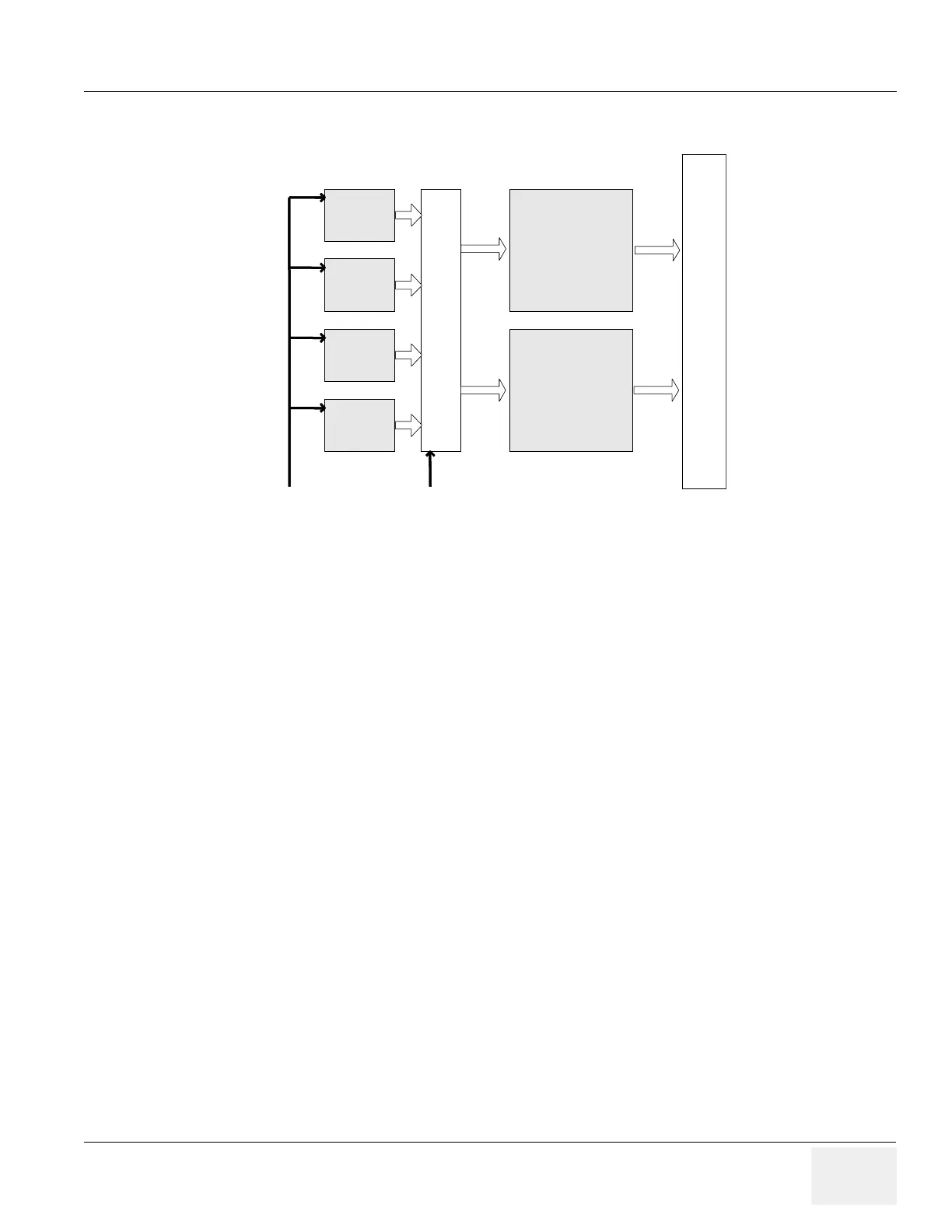
5-4-2-5 Transmit Pulse Generation Block
The CTX in CL1TRX generate bipolar transmit pulse and have dual driver for each scan mode, for
example, low voltage driver for PWD or CFM and high voltage for B. This board has 64 channels
transmit signal drivers, Transmit Pulse Generator ASIC, control FPGA and so on. Transmit pulse are
generated by TPG2 ASIC. Each TPG2 ASIC makes 16 channels signals, so total 4 ASIC are used in
CTX in CL1TRX. All of control informations for pulse generation, pulse width, time delay of each channel
are come from SYSCONPM(SYSCONCM) in real time via Backplane. The control FPGA, TRBC FPGA
provide interface between SYSCONPM(SYSCONCM) and TPG2 ASICs and control operation
condition of CTX in CL1TRX Main items are
• TPG2 ASIC: A TPG2 ASIC can generate 16 channels logic level transmit pulse signal. This ASIC
use 2 phase 40MHz clocks for transmit delay control and pulse generation. 40Mhz operation clocks
are come from L1SYSCON assy via Backplane.
• Transmit Pulse Driver : TPG2 ASIC generated logic level signal for transmit pulse. So this signal
need to be expanded to high voltage signal. Driver circuit make logic level signal to high voltage
level signal.
• THV Switch : LOGIQ™ P5 system use dual transmit high voltage for transmit driver because B
mode and CFM mode use different voltage level of transmit pulse. So in duplex of triplex mode, B/
CFM or B/DOP, Low THV and High THV are switched in CTX in CL1TRX in real time.
• TRBC FPGA : This FPGA is located on L1BFC board interfacing with SYSCONPM(SYSCONCM)
and updating the TPG data in real time.
Figure 5-14 Tx pulse Generation Block Diagram
TPG2
TX Dri ver_HVL
(CTX Only)
TX Dri ver_HVH
Selection Buffer
TPG2
TPG2
TPG2
64ch
TX signal
for HVL
64ch
TX signal
for HVH
TPG2
Control Signal
Probe Interface Board
Buffer enable signal
to select TX Dri ver
TPG2
TX Dri ver_HVL
(CTX Only)
TX Dri ver_HVH
Selection Buffer
TPG2
TPG2
TPG2
64ch
TX signal
for HVL
64ch
TX signal
for HVH
TPG2
Control Signal
Probe Interface Board
Buffer enable signal
to select TX Dri ver
 Loading...