i-
Detector Mode
SAMPLE
POS PEAK
NEG PEAK
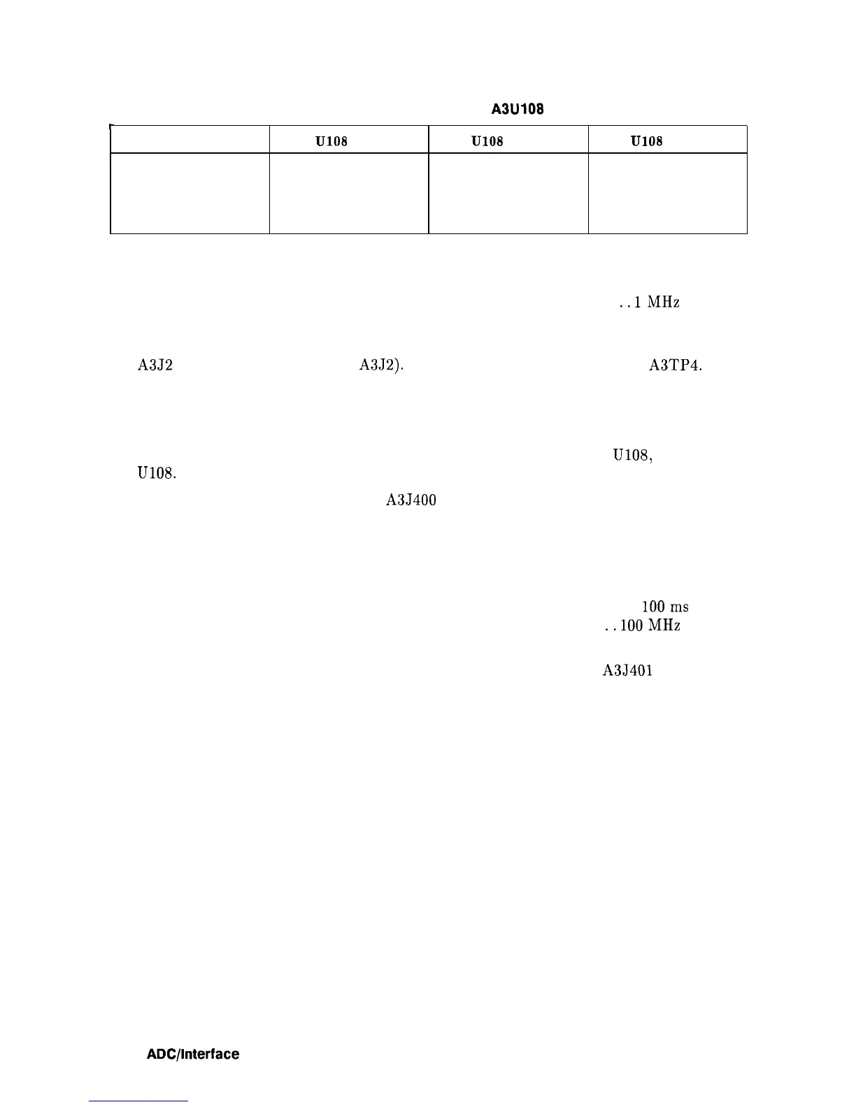
Table 7-9. Logic Levels at
A3U108
U108 pin 1
U108
pin 15
U108
pin 16
H
L
H
H L
L
L
H H
5. Set the HP 8560A to the following settings:
SPAN
. . . . . . . . . . . . . . . . . . . . . . . . . . . . . . . . . . . . . . . . . . . . . . . . . . . . . . . .
..lMHz
SWEEP TIME
. . . . . . . . . . . . . . . . . . . . . . . . . . . . . . . . . . . . . . . . . . . . . . . . . . 50ms
6. Check for the presence of the SCAN RAMP signal by connecting an oscilloscope probe to
A3J2 pin 45 (
component side of
A3J2).
Connect the negative-probe lead to
A3TP4.
7. A 0 to 10 V ramp should be present in both LINE and FREE RUN trigger modes. If the
waveform is present only in LINE trigger, ADC control signal HBADC-CLKO may be
faulty. Refer to “ADC Control Signals” in this chapter.
8. If the scan ramp is present, but is not being switched to the output of U108, replace
U108.
If the scan ramp is absent in either mode, do the following:
a. Connect the oscilloscope probe to A3J400 pin 15 (HSCAN).
b. A TTL signal (high during 50 ms sweep time and low during retrace) should
be present, indicating A3 is working properly. Refer to the Synthesizer Section
troubleshooting procedure.
A faulty TTL signal indicates a bad A3 Interface assembly.
9. Set the HP 8560A to the following settings:
SWEEP TIME
. . . . . . . . . . . . . . . . . . . . . . . . . . . . . . . . . . . . . . . . . . . . . . . . .
100ms
SPAN
. . . . . . . . . . . . . . . . . . . . . . . . . . . . . . . . . . . . . . . . . . . . . . . . . . . . . .
..lOOMHz
IF Adjust . . . . . . . . . . . . . . . . . . . . . . . . . . . . . . . . . . . . . . . . . . . . . . . . . . . . . . . . . ON
10. Check for the presence of the CAL OSC TUNE signal by monitoring A3J401 pin 25 with
an oscilloscope. If ERR 499 CAL UNLK is displayed and a signal greater than 10 V
peak-to-peak during part of the retrace period, is present, the fault is on the A3 assembly.
11. If a constant dc voltage is present during the sweep and all of the retrace period, refer to
the IF Section troubleshooting procedure.
7-20
ADC/lnterface
Section