13. Monitor A3U401 pin 9 (LV_STB) with an oscilloscope or logic probe. This is the strobe
for the A4 Log Amplifier/Cal Oscillator assembly.
14. Press
[w)
and check that pulses occur when toggling between LINEAR and
LOG DB/DIV .
Interface Strobe Select
See function block K of A3 Interface Assembly Schematic Diagram (sheet 3 of 6).
Interface strobe select generates the various strobes used by circuits on the A3 Interface
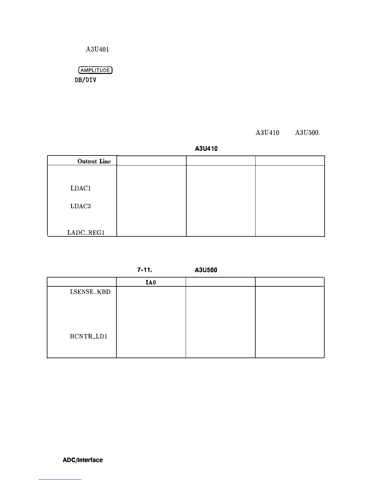
Assembly. Tables 7-10 and 7-11 are the truth tables for demultiplexers
A3U410 and A3U500.
Table 7-10. Demultiplexer A3U410 Truth Table
Selected
Outmt
he
Pin
15,
LSCAN_KBD
Pin 14, not used
Pin
13,
LDACl
Pin
12,
LDAC2
Pin
11,
LDACS
Pin 10, not used
Pin 9, not used
Pin 7,
LADC-REGl
IA1
IA2 IA3
L
L
L
H
L
L
L
H
L
H
H
L
L
L
H
H
L
H
L
H
H
H
H H
Table 7-11. Demultiplexer A3U500 Truth Table
Selected Output Line
IA0
IA1
IA2
Pin 15,
LSENSE-KBD
L L
L
Pin 14, LINT_PRIOR
H L
L
Pin 13, LADC_DATA1
L H
L
Pin 12, LDAC_DATA0
H
H
L
Pin 11, HCNTR_LDO
L
L
H
Pin 10,
HCNTR-LDl
H L
H
Pin 9, LRPG_RD
L H
H
Pin 7, LADC_REGO
H
H
H
7-28
ADC/lnterface
Section