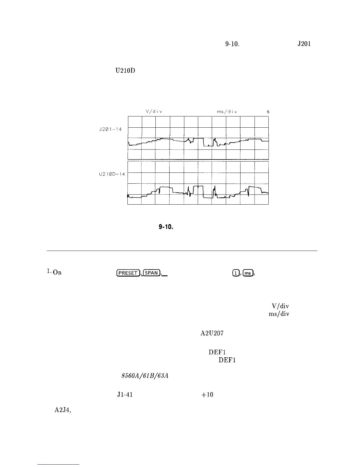
9. The waveforms should look like those illustrated in Figure
9-10.
If the waveform at
J201
pin 14 is bad, troubleshoot the Y Line Generator (function block I of A2 Controller
Schematic, sheet 1 of 4 in the Component-Level Information binder).
10. If the waveform at U210D pin 14 is bad, troubleshoot the Z Output circuit (function block
M of A2 Controller Schematic, sheet 1 of 4).
11. Remove the jumpers.
10.0
V,‘dlv
0.00 v 1.00
ms/div
0.000 s
J201-14
U210D-14
SK199
Figure 9-10. Delta Y Waveform
Analog Zero-Span Problems
l.
On the HP 8560A press
(PRESET),
(m),
ZERO SPAN , (SWEEP),
0,
[ms, (CAL), MORE, and
CRT ADJ PATTERN.
2. Set an oscilloscope to the following settings:
Amplitude scale
. . . . . . . . . . . . . . . . . . . . . . . . . . . . . . . . . . . . . . . . . . . . . . . . 10
V/div
Sweep time
. . . . . . . . . . . . . . . . . . . . . . . . . . . . . . . . . . . . . . . . . . . . . . . . . . . . 1
ms/div
Triggering
. . . . . . . . . . . . . . . . . . . . . . . . . . . . . . . . . . . . . . . . . . . . . . . . . . . ..External
3. Externally trigger the oscilloscope off the signal at A2U207 pin 8 (LBRIGHT).
4. The display should be similar to Figure 9-11 except that the untriggered trace should
show at the left edge of the screen. In these settings,
DEFl
causes switching between the
line generators and the analog inputs (sweep and video).
DEFl
remains high when the
CRT adjust pattern is on. Refer to function block M of the A2 Controller Schematic,
sheet 1 of 4 in the HP
856OA/61B/63A
Spectrum Analyzer Component Level Information
binder.
5. The sweep input from
51-41
should go from 0 V to
+lO
V; the Video In signal should go
from about 0 V to 1 V from the bottom to the top of the screen. Apply a dc voltage to
A2J4,
Video In, to test the circuit.
9-12 Controller Section