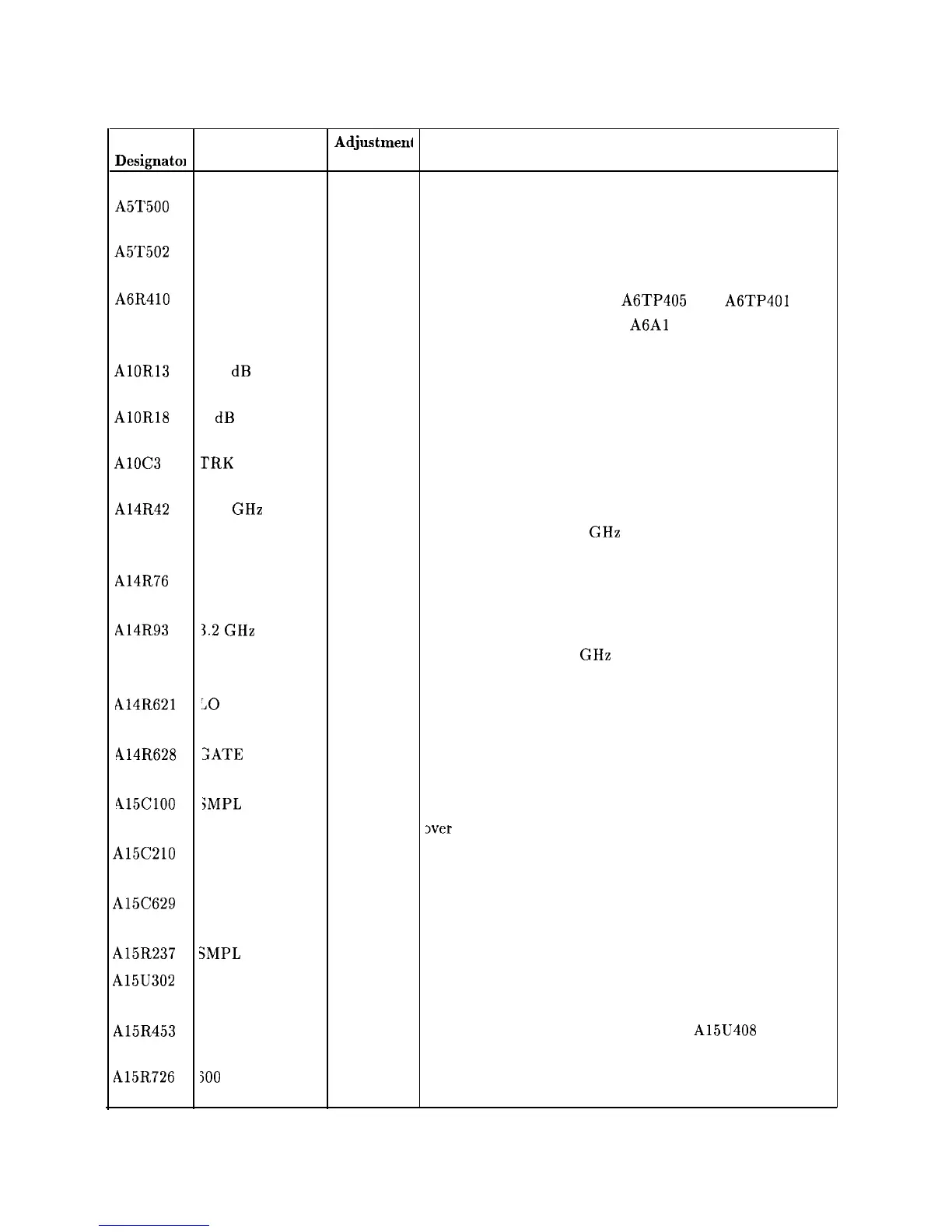
Table 2-2. Adjustable Components (2 of 3)
Reference
Designatol
A5T500
A5T502
A6R410
AlOR
AlOR
AlOC3
A14R42
A14R76
A14R93
A14R621
414R628
415ClOO
A15C210
A15C629
A15R237
A15U302
A15R453
A15R726
Adjustment
Name
Adjustmend
Number
XTAL CTR 3
3
XTAL CTR 4
3
HV ADJ
1
-10 dB ADJ
9
3 dB ADJ
9
TRK
OSC CTR
20
5.01 GHz
7
FM SPAN
7
3.2
GHz
7
;O
AMPTD
8
>ATE BIAS
8
;MPL
MATCH 1
6
VCO RANGE
6
298 MHz ADJ
17
SMPL PWR ADJ
6
10 MHz ADJ
12
PHASE DET
BIAS
500
MHz
4MPLITUDE
6
18
Description
Adjusts center frequency of third stage of crystal
bandwidth filter to 10.7 MHz.
Adjusts center frequency of fourth stage of crystal
bandwidth filter to 10.7 MHz.
Adjusts the voltage between
A6TP405
and A6TP401
to the voltage marked on the
A6Al
High Voltage
Module.
Offsets power level range of A10 Tracking
Generator.
Adjusts gain of power level range of A10
Tracking Generator.
Centers range of A10 Tracking Generator’s
tracking oscillator.
Adjusts the main coil tune driver current at a
YTO frequency of 6.01 GHz (near the upper YTO
frequency limit).
Adjusts the FM span accuracy by affecting the
sensitivity of the FM coil driver.
Adjusts the main coil fixed driver current at a
YTO frequency of 3.2 GHz (near the lower
YTO frequency limit).
Adjusts the amplitude of the first LO by changing
the reference voltage for the leveling loop.
Adjusts the gate bias for the A7 LO Distribution
Amplifier.
Transforms the sampler input impedance to 50 ohms
3ver
the 280 to 298 MHz range.
Adjusts the VCO tank capacitance so that 21 V
on the VCO tune line equals 298 MHz VCO frequency.
Fine adjusts the 298 MHz SIG ID Oscillator
frequency to optimize its performance.
Adjusts the signal power level to the Sampler.
Adjusts frequency of the temperature
compensated crystal oscillator (TCXO) to 10 MHz.
Adjusts bias at pin 3 of phase detector A15U408 to
1.80 V.
Adjusts input power to ECL divide-by-two chip.
Adjustment Procedures 2-7