8
8-29
INPUT/OUTPUT PORTS AND PIN FUNCTIONS
32180 Group User’s Manual (Rev.1.0)
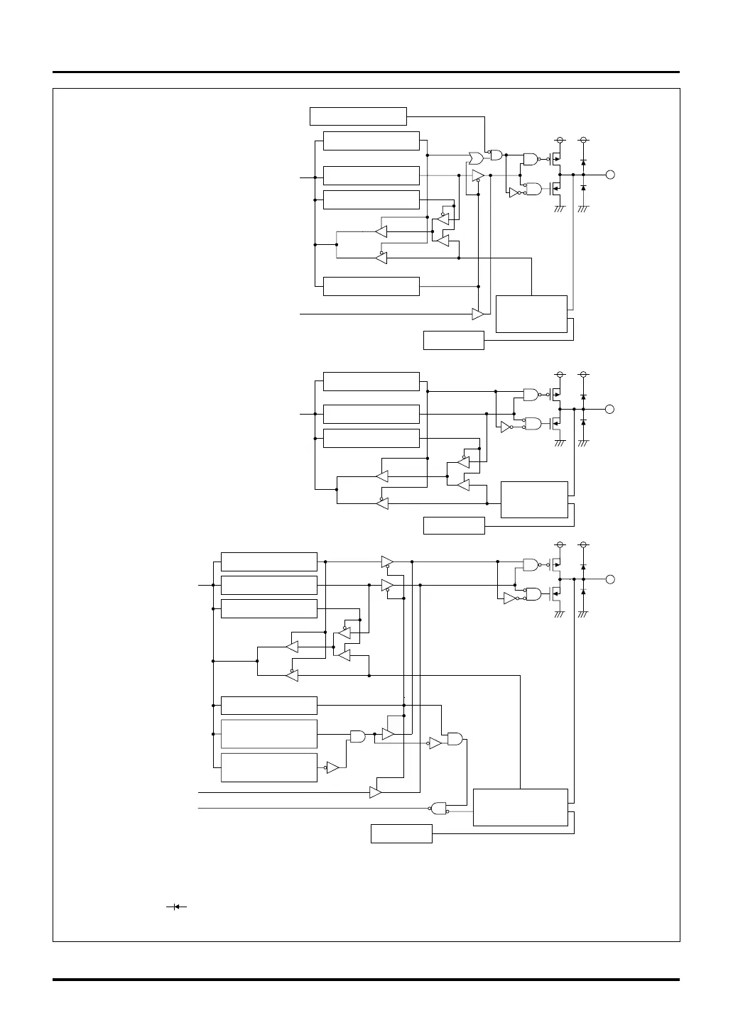
8.5 Port Peripheral Circuits
Data bus
Input data select bit
UART/CSIO function
select bit
Internal/external clock
select bit
SCLKOi
output
SCLKIi input
Port level switching
function (Standard:
peripheral Schmitt)
Port level switching
function (No
peripheral input)
P65(SCLKI4/SCLKO4)
P66(SCLKI5/SCLKO5)
P84(SCLKI0/SCLKO0)
P87(SCLKI1/SCLKO1)
P41(BLW#/BLE#)
P42(BHW#/BHE#)
P43(RD#)
P61–P63
P67
Data bus
(Note 1)
(Note 1)
P160–P165(TO21–TO26)
P180–P185(TO29–TO34)
P210–P215(TO37–TO42)
Data bus
Operation mode register
Input function
enable
Peripheral function output
Port output latch
Direction register
Input data select bit
Port level switching
function (No
peripheral input)
(Note 1)
PWM output disable
Note 1: For details about the port level switching function, see Section 8.4, "Port Input Level Switching Function."
Notes: • During processor and external extension modes, P41-P43 are external bus interface control signal pins, but their
functional description in this block diagram is omitted.
• The circle denotes a pin.
• The symbol denotes a parasitic diode. Make sure the voltage applied to each pin does not exceed the VCCE voltage.
• The input capacitance of each pin is approximately 10 pF.
Input function
enable
Port output latch
Direction register
Input data select bit
Port output latch
Direction register
Input function
enable
Operation mode register
Figure 8.5.3 Port Peripheral Circuit Diagram (3)

 Loading...


