10
10-25
MULTIJUNCTION TIMERS
10.2 Common Units of Multijunction Timers
32180 Group User’s Manual (Rev.1.0)
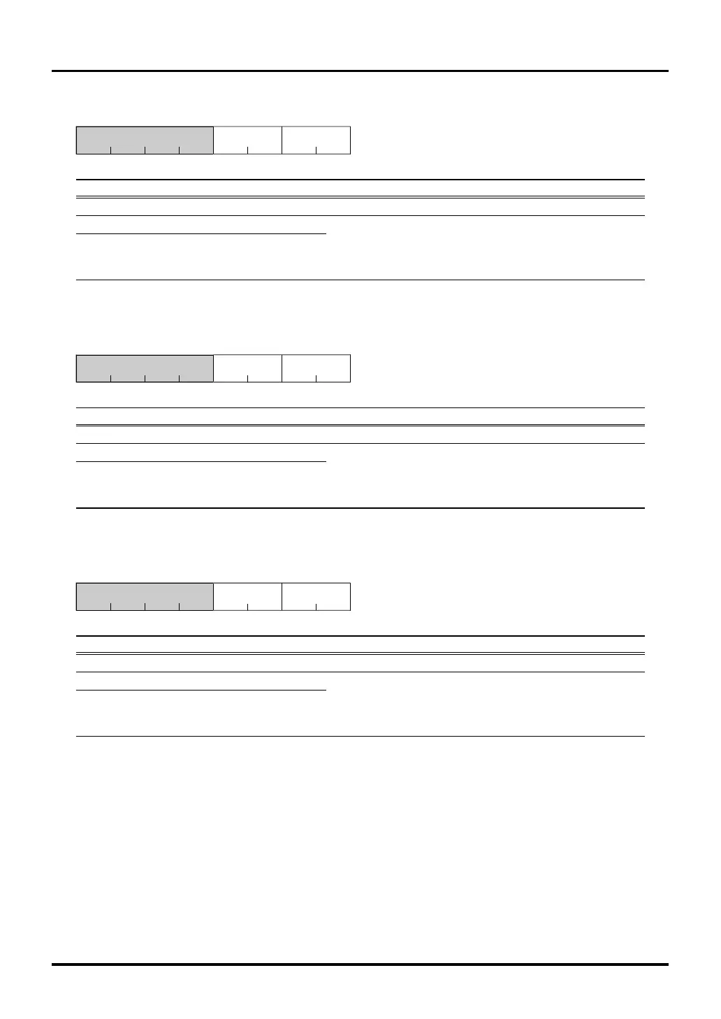
TIN24, 25 Input Processing Control Register (TIN2425CR) <Address: H’0080 07E1>
9 1011121314
b15
b8
TIN24STIN25S
0000
<After reset: H’00>
b Bit Name Function R W
8–11 No function assigned. Fix to "0". 00
12, 13 TIN25S (TIN25 input processing select bit) 00: Disable input R W
14, 15 TIN24S (TIN24 input processing select bit) 01: Rising edge
10: Falling edge
11: Both edges
TIN26, 27 Input Processing Control Register (TIN2627CR) <Address: H’0080 0BE1>
9 1011121314b15b8
TIN26STIN27S
0000
<After reset: H’00>
b Bit Name Function R W
8–11 No function assigned. Fix to "0". 00
12, 13 TIN27S (TIN27 input processing select bit) 00: Disable input R W
14, 15 TIN26S (TIN26 input processing select bit) 01: Rising edge
10: Falling edge
11: Both edges
TIN28, 29 Input Processing Control Register (TIN2829CR) <Address: H’0080 0CE1>
9 1011121314b15b8
TIN28STIN29S
0000
<After reset: H’00>
b Bit Name Function R W
8–11 No function assigned. Fix to "0". 00
12, 13 TIN29S (TIN29 input processing select bit) 00: Disable input R W
14, 15 TIN28S (TIN28 input processing select bit) 01: Rising edge
10: Falling edge
11: Both edges

 Loading...


