10
10-24
MULTIJUNCTION TIMERS
10.2 Common Units of Multijunction Timers
32180 Group User’s Manual (Rev.1.0)
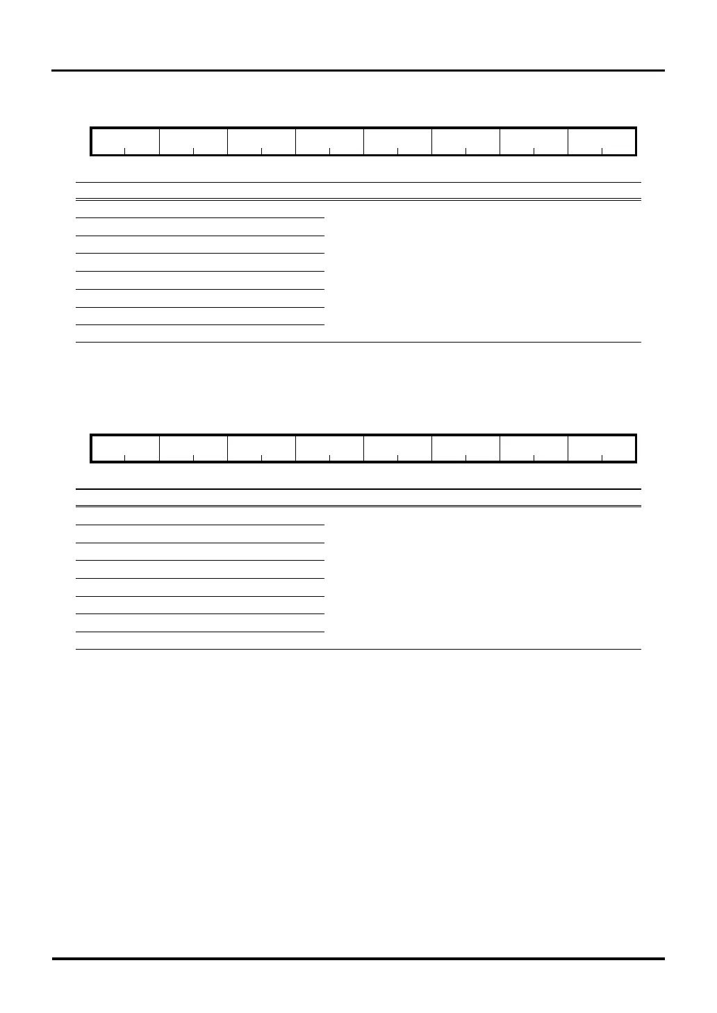
TIN12–19 Input Processing Control Register (TIN1219CR) <Address: H’0080 0218>
b01234567891011121314b15
TIN19S TIN18S TIN17S TIN16S TIN15S TIN14S TIN13S TIN12S
0000000000000000
<After reset: H’0000>
b Bit Name Function R W
0, 1 TIN19S (TIN19 input processing select bit) 00: Disable input R W
2, 3 TIN18S (TIN18 input processing select bit) 01: Rising edge
4, 5 TIN17S (TIN17 input processing select bit) 10: Falling edge
6, 7 TIN16S (TIN16 input processing select bit) 11: Both edges
8, 9 TIN15S (TIN15 input processing select bit)
10, 11 TIN14S (TIN14 input processing select bit)
12, 13 TIN13S (TIN13 input processing select bit)
14, 15 TIN12S (TIN12 input processing select bit)
Note: • This register must always be accessed in halfwords.
TIN20–23, TIN30–33 Input Processing Control Register (TIN2023_3033CR) <Address: H’0080 021A>
b01234567891011121314b15
TIN33S TIN32S TIN31S TIN30S TIN23S TIN22S TIN21S TIN20S
0000000000000000
<After reset: H’0000>
b Bit Name Function R W
0, 1 TIN33S (TIN33 input processing select bit) 00: Disable input R W
2, 3 TIN32S (TIN32 input processing select bit) 01: Rising edge
4, 5 TIN31S (TIN31 input processing select bit) 10: Falling edge
6, 7 TIN30S (TIN30 input processing select bit) 11: Both edges
8, 9 TIN23S (TIN23 input processing select bit)
10, 11 TIN22S (TIN22 input processing select bit)
12, 13 TIN21S (TIN21 input processing select bit)
14, 15 TIN20S (TIN20 input processing select bit)
Note: • This register must always be accessed in halfwords.

 Loading...


