EasyManua.ls Logo

Renesas M32R/ECU Series User Manual

Renesas M32R/ECU Series
839 pages
To Next Page IconTo Next Page
To Previous Page IconTo Previous Page
Page #452 background imageLoading...
Page #452 background image
11
11-7
A-D Converters
32180 Group User's Manual (Rev.1.0)
A-D conversion interrupt or DMA transfer request
ADiIN0
Completed here when operating
in single-shot scan mode
ADiDT0
10-bit A-Di Data Register
Conversion
starts
(Note 1)
ADiIN1
ADiINn-1
ADiINn
ADiDT1 ADiDTn-1 ADiDTn
During continuous scan mode
<n-channel scan>
i=0, 1
n=0–15
Note 1: A-D0 conversion start: Software trigger Started by setting the A-D0 conversion start bit to "1"
Hardware trigger Started by input event bus 3, input event bus 2,
output event bus 3 or TIN23S signal input
A-D1 conversion start: Software trigger Started by setting the A-D1 conversion start bit to "1"
Hardware trigger Started by input event bus 3, input event bus 2,
TID1_udf/ovf or TIN23S signal input
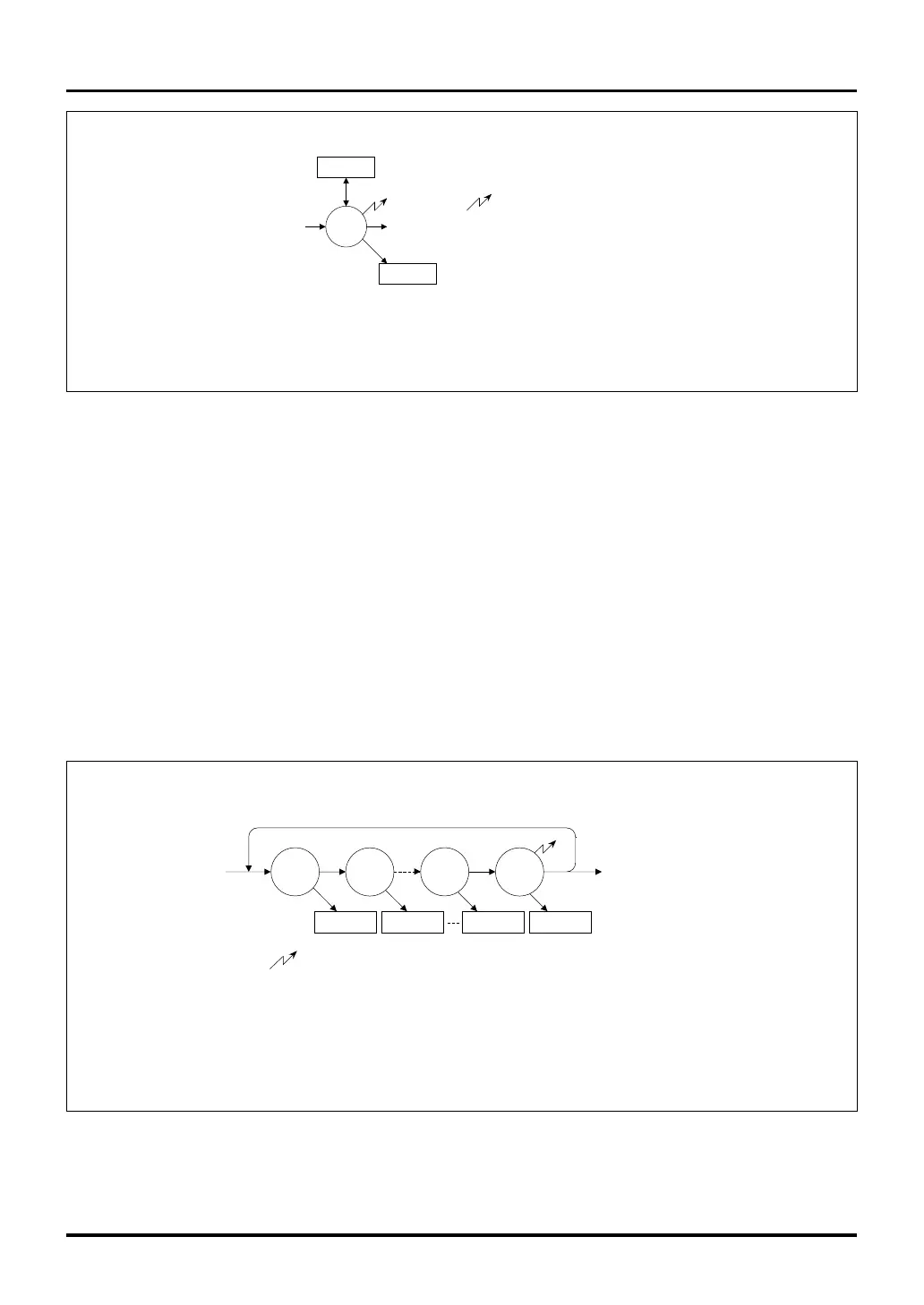
Figure 11.1.5 Operation of A-D Conversion in Scan Mode
11.1 Outline of A-D Converters
Figure 11.1.4 Operation in Single Mode (Comparate)
(2) Scan Mode
In scan mode, the analog input voltages on two or more selected channels from channel 0 (ADiIN0, i = 0 or 1)
to the channel (channels 015) selected by the A-D Scan Mode Register 1 scan loop select bit are sequen-
tially A-D converted.
There are two types of scan mode: Single-shot scan mode in which A-D conversion is completed after
performing one cycle of scan operation, and Continuous scan mode in which scan operation is continued
until halted by setting the A-D scan mode register 0s A-D conversion stop bit to "1".
These types of scan mode are selected using A-D Scan Mode Register 0. The channels to be scanned are
selected using A-D Scan Mode Register 1. The selected channels are scanned sequentially beginning with
channel 0.
An A-D conversion interrupt or DMA transfer request can be generated when one cycle of scan operation is
completed.
A-D conversion interrupt
or DMA transfer request
Note 1: Comparate operation is started by writing a comparison value to the Successive
Approximation Register (ADiSAR)
ADiINn
Completed
ADiCMP
A-Di Comparate
Data Register
Conversion
starts
(Note 1)
ADiSAR
A-D Successive Approximation Register
Comparate result
ADiCMP=0 (ANn > ADiSAR)
ADiCMP=1 (ANn < ADiSAR)
i=0,1
n=0–15

Table of Contents

Question and Answer IconNeed help?

Do you have a question about the Renesas M32R/ECU Series and is the answer not in the manual?

Renesas M32R/ECU Series Specifications

General IconGeneral
BrandRenesas
ModelM32R/ECU Series
CategoryComputer Hardware
LanguageEnglish

Summary

Before Use

Guide to Understanding the Register Table

Explains the conventions used in register tables, including bit numbering, register borders, status after reset, shaded bits, and read/write conditions.

CHAPTER 1 OVERVIEW

1.1 Outline of the 32180 Group

Provides an overview of the 32180 group, belonging to the M32R/ECU series of Mitsubishi microcomputers.

1.3 Pin Functions

Describes the functions of each pin on the 32180, including primary and alternative functions.

1.4 Pin Assignments

Provides the pin assignment diagram and table for the 240QFP package.

CHAPTER 4 EIT

4.2 EIT Events

Details the types of exceptions (RIE, AE, FPE), underflow, inexact, and zero division exceptions.

CHAPTER 5 INTERRUPT CONTROLLER (ICU)

5.2 ICU Related Registers

Shows a register map associated with the Interrupt Controller (ICU), including Interrupt Vector Register and Interrupt Request Mask Register.

CHAPTER 6 INTERNAL MEMORY

6.1 Outline of the Internal Memory

Details the types of memory contained within the 32180: 48-Kbyte RAM and 1-Mbyte flash memory.

6.5 Programming the Internal Flash Memory

Explains the methods for programming or erasing the internal flash memory, including boot mode and single-chip mode.

CHAPTER 7 RESET

7.1 Outline of Reset

Describes the microcomputer reset mechanism via the RESET# input pin and the execution from the reset vector entry.

7.2 Reset Operation

Details reset operations such as power-on reset, reset during operation, reset at entering RAM backup mode, and reset vector relocation during flash programming.

CHAPTER 8 INPUT/OUTPUT PORTS AND PIN FUNCTIONS

8.1 Outline of Input/Output Ports

Details the total number of input/output ports and their dual/triple function capabilities.

8.2 Selecting Pin Functions

Explains how pin functions are selected based on the current operation mode or by setting port operation mode registers.

8.3 Input/Output Port Related Registers

Lists the port data registers, port direction registers, and port operation mode registers.

CHAPTER 9 DMAC

9.2 DMAC Related Registers

Shows a memory map of the DMAC related registers, including channel control, source address, and destination address registers.

CHAPTER 10 MULTIJUNCTION TIMERS

10.1 Outline of Multijunction Timers

Introduces the multijunction timers (MJT), their input/output event buses, and the six types of MJT provided.

10.2 Common Units of Multijunction Timers

Details the common units within MJTs: Prescaler, Clock Bus, Input/Output Event Bus Control, Input Processing, Output Flip-flop, and Interrupt Control Units.

10.3 TOP (Output-Related 16-Bit Timer)

Describes the TOP timer, its specifications, modes of operation (single-shot, delayed, continuous), and interrupt generation.

CHAPTER 11 A-D CONVERTERS

11.2 A-D Converter Related Registers

Shows the A-D converter related register map, including single mode, scan mode, and data registers.

11.3 Functional Description of A-D Converters

Explains how to find analog input voltages, A-D conversion by successive approximation, comparator operation, and conversion time.

CHAPTER 12 SERIAL I/O

12.2 Serial I/O Related Registers

Shows the serial I/O related register map, including interrupt and buffer registers.

CHAPTER 13 CAN MODULE

13.2 CAN Module Related Registers

Provides the CAN module related register map, covering control, status, frame format, and mask registers.

CHAPTER 14 REAL TIME DEBUGGER (RTD)

14.1 Outline of the Real-Time Debugger (RTD)

Explains the RTD as a serial I/O for reading/writing internal RAM locations via external commands without stopping the CPU.

14.3 Functional Description of the RTD

Details RTD operations for commands like VER, VEI, RDR, WRR, and RCV.

CHAPTER 15 EXTERNAL BUS INTERFACE

15.2 External Bus Interface Related Registers

Shows the register map for the external bus interface, including port operation mode registers.

CHAPTER 16 WAIT CONTROLLER

16.2 Wait Controller Related Registers

Shows the Wait Controller related register map, including CS Area Wait Control Registers.

CHAPTER 17 RAM BACKUP MODE

17.1 Outline of RAM Backup Mode

Describes RAM backup mode where internal RAM contents are retained when power is off, used for power saving or when power is down.

CHAPTER 19 JTAG

CHAPTER 21 ELECTRICAL CHARACTERISTICS

21.1 Absolute Maximum Ratings

Lists the absolute maximum ratings for various parameters such as power supply, input/output voltage, and temperature.

APPENDIX 4 SUMMARY OF PRECAUTIONS

Appendix 4.4 Precautions To Be Observed when Programming Internal Flash Memory

Details precautions for programming/erasing internal flash memory, including voltage transitions and pin usage.

Related product manuals