2
2-9
32180 Group User’s Manual (Rev.1.0)
CPU
2.6 Data Formats
2.6.2 Data Formats
(1) Data formats in registers
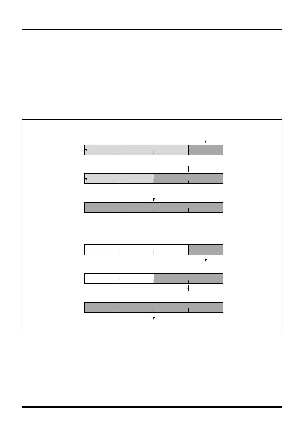
The data sizes in the M32R-FPU registers are always words (32 bits).
When loading byte (8-bit) or halfword (16-bit) data from memory into a register, the data is sign-extended
(LDB, LDH instructions) or zero-extended (LDUB, LDUH instructions) to a word (32-bit) quantity before
being loaded in the register.
When storing data from a register into a memory, the 32-bit data, the 16-bit data on the LSB side and the 8-
bit data on the LSB side of the register are stored into memory by the ST, STH and STB instructions,
respectively.
Figure 2.6.2 Data Formats in Registers
Rn
b0 b31
<Load>
Byte
Rn
b0 b31
Halfword
Rn
b0 b31
Word
Sign-extended (LDB instruction) or
zero-extended (LDUB instruction)
From memory
(LDB, LDUB instructions)
<Store>
Rn
b0 b31
Byte
Rn
b0 b31
Halfword
Rn
b0 b31
Word
To memory (STB instruction)
To memory (STH instruction)
To memory (ST instruction)
From memory (LDH, LDUH instructions)
From memory (LD instruction)
Sign-extended (LDH instruction) or
zero-extended (LDUH instruction)
24
16
24
16

 Loading...


