3.1.2. ATX PLL
The ATX PLL contains LC tank-based voltage controlled oscillators (VCOs). These LC
VCOs have different frequency ranges to support a continuous range of operation.
When driving the transceiver directly, the ATX PLL only supports the integer mode.
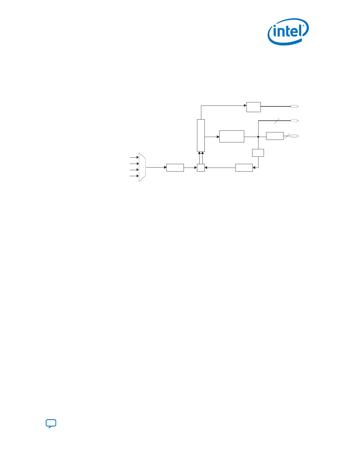
Figure 119. ATX PLL Block Diagram
VCO
Lock
Detector
PFD
CP &
LF
Refclk
Multiplexer
2
2
/2
M CounterN Counter
L Counter
Reference clock network
M Counter
Receiver input pin
Dedicated reference clock pin
DownUp
Global clock or core clock
pll_locked
refclk
fbclk
Input reference
clock
Input Reference Clock
This is the dedicated input reference clock source for the PLL.
The input reference clock can be sourced from one of the following:
• Dedicated reference clock pin
• Reference clock network
• Receiver input pin
• Global clock or the core clock network
The input reference clock to the dedicated reference clock pin is a differential signal.
Intel recommends using the dedicated reference clock pin as the input reference clock
source for the best jitter performance. The input reference clock must be stable and
free-running at device power-up for proper PLL operation and PLL calibration. If the
reference clock is not available at device power-up, then you must recalibrate the PLL
when the reference clock is available.
Note: The ATX PLL calibration is clocked by the CLKUSR clock which must be stable and
available for calibration to proceed. Refer to the Calibration section for more details
about the CLKUSR clock.
Reference Clock Multiplexer
The reference clock (refclk) multiplexer selects the reference clock to the PLL from
the various reference clock sources available.
N Counter
The N counter divides the refclk mux's output. The division factors supported are 1,
2, 4, and 8.
3. PLLs and Clock Networks
UG-20070 | 2018.09.24
Send Feedback
Intel
®
Cyclone
®
10 GX Transceiver PHY User Guide
201