3.2. Input Reference Clock Sources
The transmitter PLL and the clock data recovery (CDR) block need an input reference
clock source to generate the clocks required for transceiver operation. The input
reference clock must be stable and free-running at device power-up for proper PLL
calibrations.
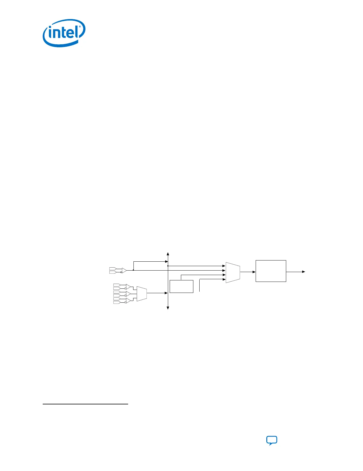
Cyclone 10 GX transceiver PLLs have five possible input reference clock sources,
depending on jitter requirements:
• Dedicated reference clock pins
• Reference clock network
• The output of another fPLL with PLL cascading
• Receiver input pins
• Global clock or core clock
(28)
For the best jitter performance, Intel recommends placing the reference clock as close
as possible to the transmit PLL. For protocol jitter compliance at a data rate > 10
Gbps, place the reference clock pin in the same triplet as the transmit PLL. The
following protocols require the reference clock to be placed in same bank as the
transmit PLL:
• OC-192 and 10 GPON
Note: For optimum performance, the reference clock of transmit PLL is recommended to be
from a dedicated reference clock pin in the same bank.
Figure 122. Input Reference Clock Sources
Dedicated
refclk
pin
RX pin 2
RX pin 1
Note : (1) You can choose only one of the three RX pins to be used as an input reference clock source. Any RX pin on the same side
of the device can be used as an input reference clock.
RX pin 0
Reference Clock
Network
Serial Clock
fPLL
fPLL
Input
Reference
Clock
(2)
(3)
(2) Dedicated refclk pin can be used as an input reference clock source only for ATX or fPLL or to the reference clock network.
Reference clock network can then drive the CMU PLL.
(3) The output of another PLL can be used as an input reference clock source during PLL cascading. Cyclone 10 GX transceivers support fPLL to fPLL cascading.
(1)
Global or
Core Clock
Note: To successfully complete the calibration process, the reference clocks driving the PLLs
(ATX PLL, fPLL, CDR/CMU PLL) must be stable and free running at start of FPGA
configuration. Otherwise, recalibration will be necessary.
(28)
Not available for CMU.
3. PLLs and Clock Networks
UG-20070 | 2018.09.24
Intel
®
Cyclone
®
10 GX Transceiver PHY User Guide
Send Feedback
208