5.3.1. Transmitter Datapath
5.3.1.1. TX FIFO (Shared with Enhanced PCS and PCIe Gen2 PCS)
The TX FIFO interfaces between the transmitter PCS and the FPGA fabric and ensures
reliable transfer of data and status signals. It compensates for the phase difference
between the FPGA fabric clock and tx_clkout (the low-speed parallel clock). The TX
FIFO has a depth of 8 and operates in low latency mode, register mode, and fast
register mode.
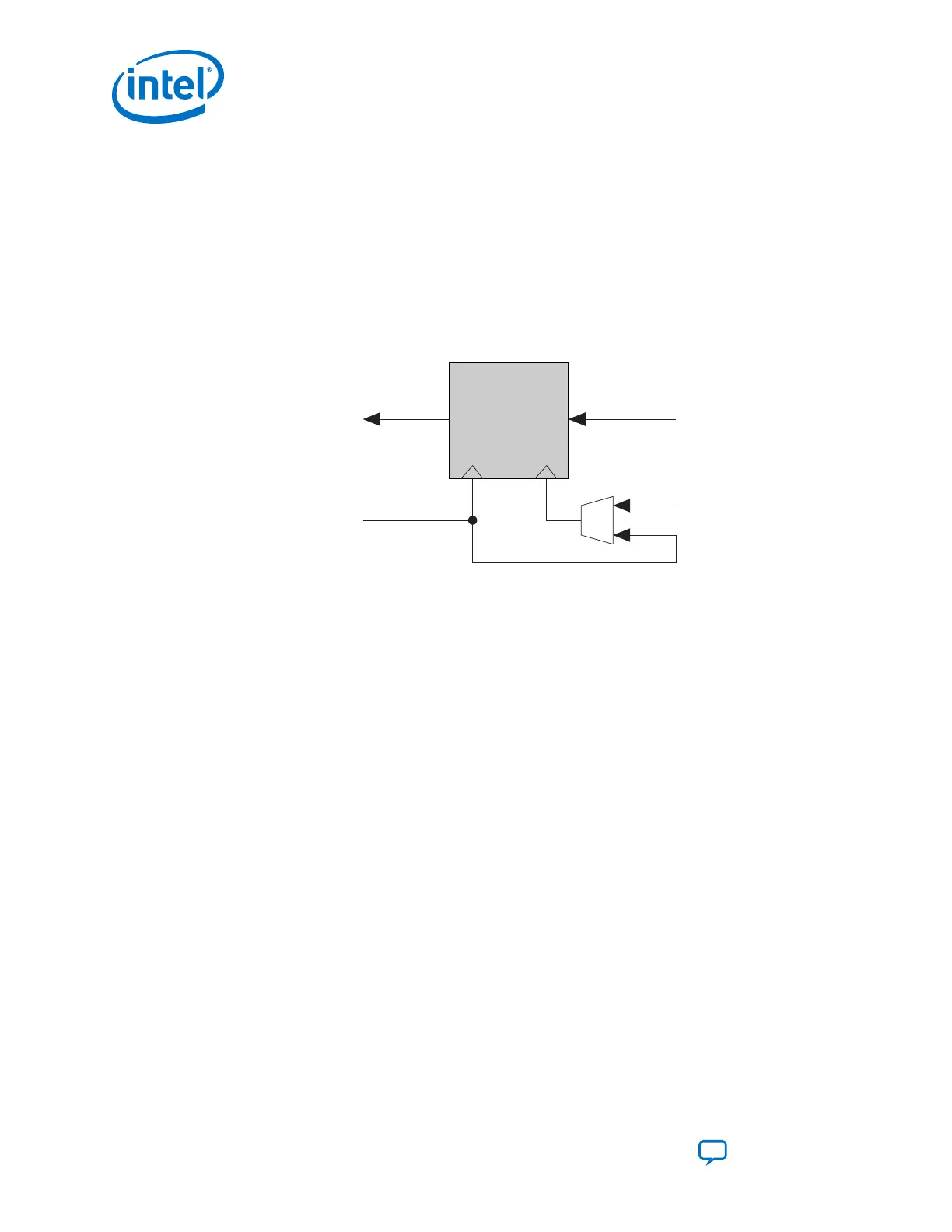
Figure 196. TX FIFO Block Diagram
TX
FIFO
Datapath from FPGA Fabric
or PIPE Interface
tx_coreclkin
tx_clkout
Datapath to Byte Serializer,
8B/10B Encoder,
or Serializer
wr_clkrd_clk
You can control the write port using tx_clkout or tx_coreclkin. Use the
tx_clkout signal for a single channel and tx_coreclkin when using multiple
channels. The TX FIFO is shared with PCIe Gen2 and Enhanced PCS data paths.
5.3.1.1.1. TX FIFO Low Latency Mode
The low latency mode incurs two to three cycles of latency (latency uncertainty) when
connecting it with the FPGA fabric. The FIFO empty and the FIFO full threshold values
are made closer so that the depth of the FIFO decreases, which in turn decreases the
latency.
5.3.1.1.2. TX FIFO Register Mode
The register mode bypasses the FIFO functionality to eliminate the FIFO latency
uncertainty for applications with stringent latency requirements. This is accomplished
by tying the read clock of the FIFO with its write clock. The register mode incurs only
one clock cycle of latency when interfacing to the FPGA fabric.
5.3.1.1.3. TX FIFO Fast Register Mode
This mode allows a higher maximum frequency (f
MAX
) between the FPGA fabric and
the TX PCS by enabling the optional fast register interface with additional latency.
5.3.1.2. Byte Serializer
In certain applications, the FPGA fabric cannot operate at the same clock rate as the
transmitter channel (PCS) because the transmitter channel is capable of operating at
higher clock rates compared to the FPGA fabric. The byte serializer allows the
transmitter channel to operate at higher data rates while keeping the FPGA fabric
interface clock rate below its maximum limit. This is accomplished by increasing the
5. Cyclone 10 GX Transceiver PHY Architecture
UG-20070 | 2018.09.24
Intel
®
Cyclone
®
10 GX Transceiver PHY User Guide
Send Feedback
300