The ATX PLL IP GUI can generate configuration files (SystemVerilog, C header or MIF)
for a given configuration. With the multi reconfiguration profile options enabled, the
ATX PLL IP Parameter Editor can produce configuration files for all of the profiles
simultaneously. In addition, by enabling the reduced reconfiguration files generation,
the IP Parameter Editor will produce a reduced configuration file by internally
comparing the corresponding parameter settings of all the profiles and identifying the
differences.
Embedded Reconfiguration Streamer
This option enables a push-button flow to reconfigure between multiple configurations
or profiles. Here are the steps to follow:
1. Multiple reconfiguration profiles creation
• In the ATX PLL IP GUI, create configurations for each profiles using the multi-
profile feature.
2. Reconfiguration report files
• The IP GUI generates the reconfiguration report files that contain parameter
and register settings for all the selected profiles. If the reduced reconfiguration
files option is selected, the IP parameter editor will compare the settings
between the profiles and generate reduced report files which only contain the
differences.
3. Select Enable embedded reconfiguration streamer logic in the GUI to
generate the following:
• Necessary HDL files to perform streaming
• The individual report files for each profile, an SystemVerilog package file with
configuration data for all the profiles concatenated together which is used to
initialize the configuration ROM
4. Generate the ATX PLL IP and control the reconfiguration streamer using the AVMM
master.
5. If you reconfigure PLL for data rate change, you must recalibrate the PLL.
Related Information
Calibration on page 373
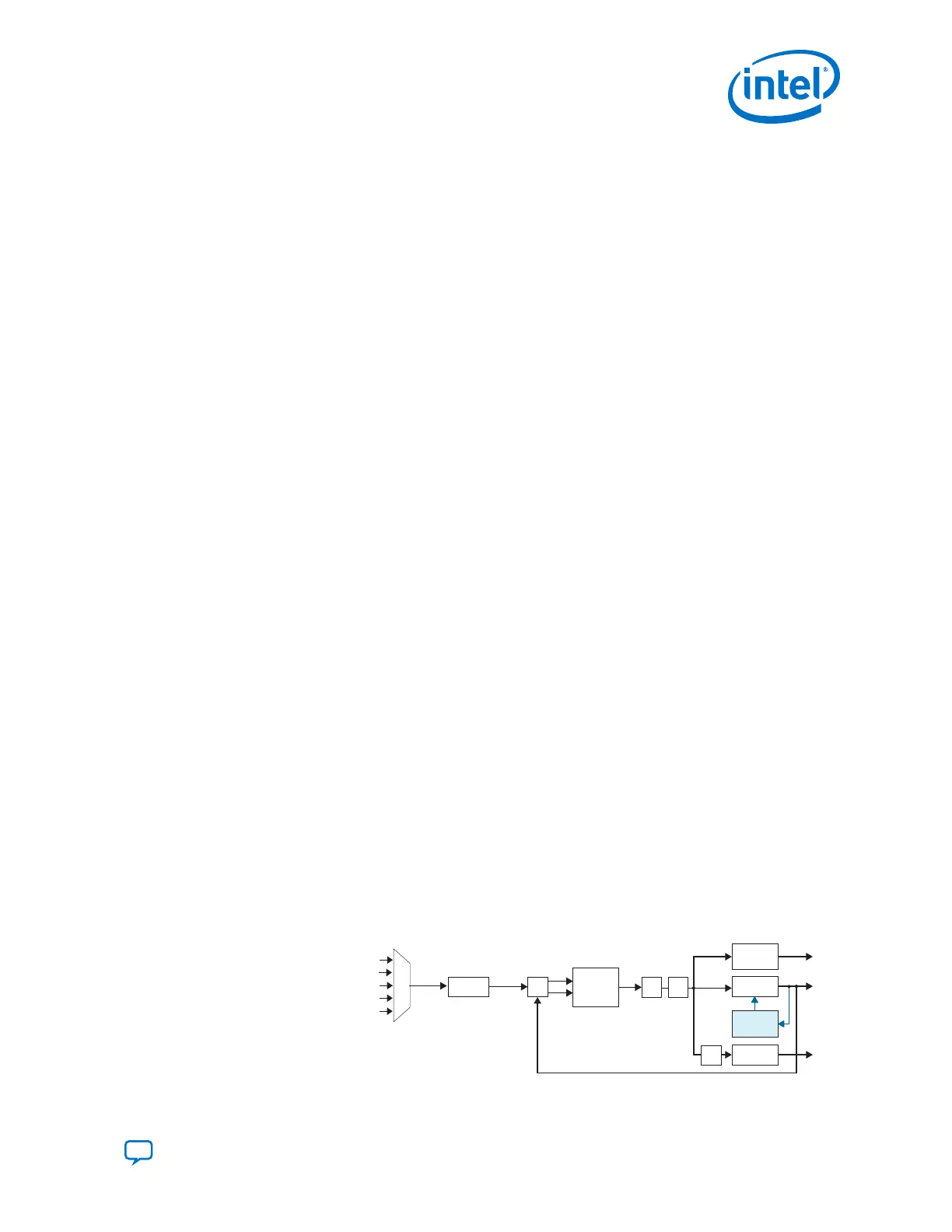
3.1.3. fPLL
There are two fPLLs in each transceiver bank with six channels (one located at the top
and the other at the bottom of the bank). Transceiver banks with three channels have
only one fPLL.
Figure 120. fPLL Block Diagram
VCO
PFD
Up
Down
Delta Sigma
Modulator
L Counter
/1, 2, 4, 8
N Counter
M Counter
Charge
Pump and
Loop Filter
C Counter
Refclk
Multiplexer
Reference Clock Network
Receiver Input Pin
Output of Another fPLL with PLL Cascading
Dedicated Reference Clock Pin
Global Clock or Core Clock
refclk
Input
Reference
Clock
fbclk
/2
/2
3. PLLs and Clock Networks
UG-20070 | 2018.09.24
Send Feedback
Intel
®
Cyclone
®
10 GX Transceiver PHY User Guide
203