Figure 176. Deserializer Block Diagram
The deserializer block sends out the LSB of the input data first.
Dn D2 D1 D0
Serial
Data
LSB
Deserializer
Parallel
Clock
Clock
Serial
Dn
D2
D1
D0
Parallel
Data
5.1.3. Loopback
The PMA supports serial, diagnostic, and reverse loopback paths.
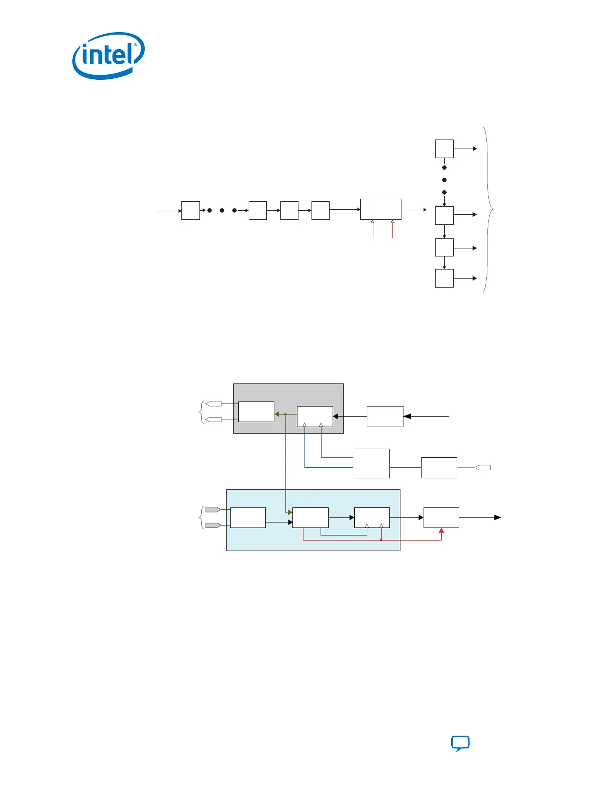
Figure 177. Serial Loopback Path
The serial loopback path sets the CDR to recover the data from serializer while data from receiver serial input
pin is ignored by CDR. The transmitter buffer sends data normally.
Transmitter
Buffer
Serial
Data
Transmitter PMA
Receiver
PCS
Deserializer
Parallel Data
to FPGA Core
Parallel
Data
Serial
Data
Serial Clock
Receiver PMA
CDR
Serial
Data
Receiver
Buffer
Parallel Clock
Serial
Loopback
Receiver Serial
Differential Input
Data
Transmitter Serial
Differential Output
Data
Transmitter
PCS
Serializer
Transmitter
PLL
Parallel Data
Parallel
from FPGA Core
Data
Serial
Clock
Input
Reference
Clock
Clock
Generation
Block
Parallel
Clock
5. Cyclone 10 GX Transceiver PHY Architecture
UG-20070 | 2018.09.24
Intel
®
Cyclone
®
10 GX Transceiver PHY User Guide
Send Feedback
282