• For ATX PLL, Read-Modify-Write 0x0 to offset address 0x110[2] of the ATX
PLL.
• For fPLL, Read-Modify-Write 0x0 to offset address 0x126[0] of the fPLL.
4. Recalibrate TX PMA of all the bonded channels driven by the ATX PLL or the fPLL.
Note: For this 10-channel example, two ATX PLLs are instantiated. Six channels of the
tx_bonding_clocks on the Native PHY IP core are connected to the first ATX PLL
and the remaining four channels are connected to the second ATX PLL's
tx_bonding_clock outputs.
Related Information
• ATX PLL Recalibration on page 385
• Fractional PLL Recalibration on page 385
• PMA Recalibration on page 386
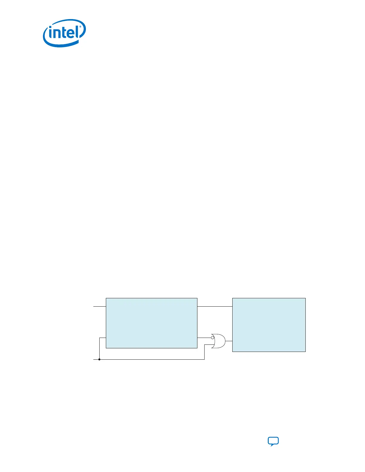
3.11.3. Implementing PLL Cascading
In PLL cascading, the output of the first PLL feeds the input reference clock to the
second PLL.
For example, if the input reference clock has a fixed frequency, and the desired data
rate was not an integer multiple of the input reference clock, the first PLL can be used
to generate the correct reference clock frequency. This output is fed as the input
reference clock to the second PLL. The second PLL generates the clock frequency
required for the desired data rate.
The transceivers in Cyclone 10 GX devices support fPLL to fPLL cascading. Only
maximum two PLLs are allowed in the cascading chain.
Note: When the fPLL is used as a cascaded fPLL (downstream fPLL), a user recalibration on
the fPLL is required. Refer to the "User Recalibration" section for more information.
Figure 145. PLL Cascading
pll_refclk0 hssi_pll_cascade_clk
pll_powerdown pll_locked
pll_refclk0
pll_powerdown
fPLL (Cascade Source) fPLL (Transceiver PLL)
Steps to implement fPLL to fPLL cascading:
1. Instantiate the fPLL IP core.
2. Set the following configuration settings for the fPLL IP core in the Parameter
Editor:
3. PLLs and Clock Networks
UG-20070 | 2018.09.24
Intel
®
Cyclone
®
10 GX Transceiver PHY User Guide
Send Feedback
240