5.3.2.7. RX FIFO (Shared with Enhanced PCS and PCIe Gen2 PCS)
The RX FIFO interfaces between the PCS on the receiver side and the FPGA fabric and
ensures reliable transfer of data and status signals. It compensates for the phase
difference between the FPGA fabric and the PCS on the receiver side. The RX FIFO has
a depth of 8. It operates in register FIFO and low latency modes.
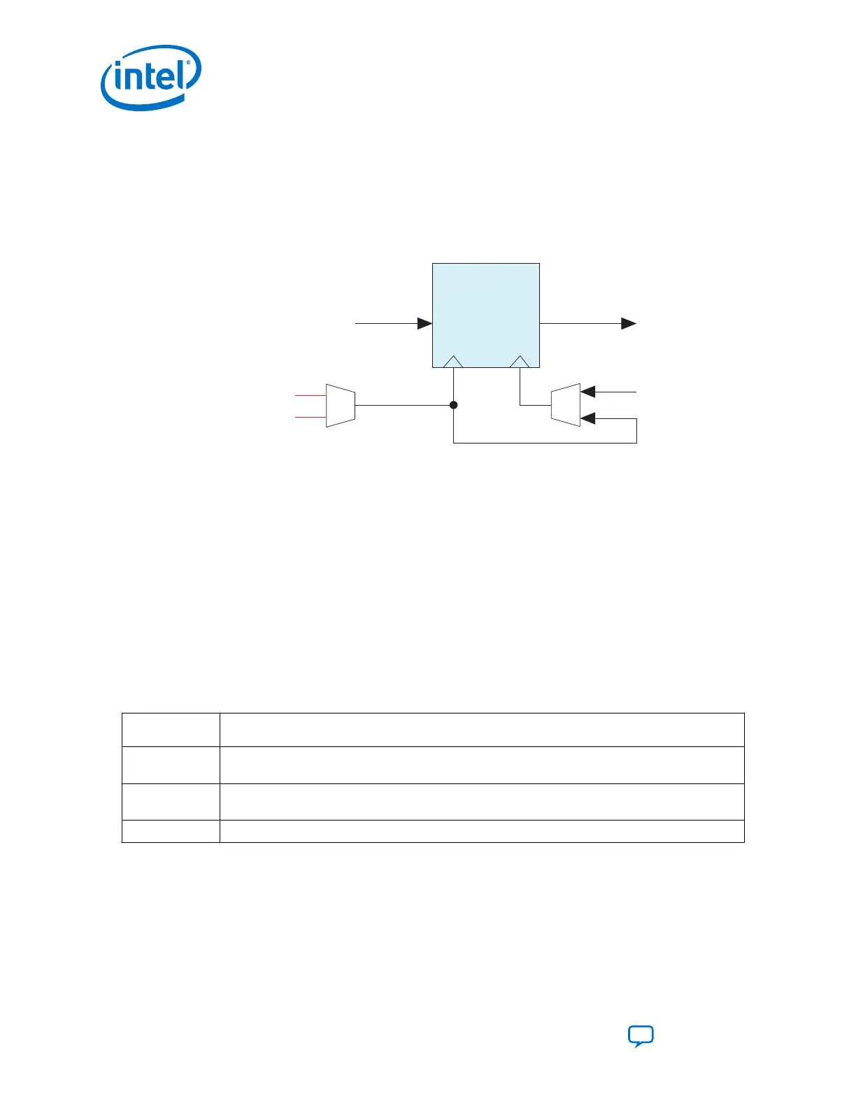
Figure 206. RX FIFO Block Diagram
RX
FIFO
Datapath to FPGA Fabric
or PIPE Interface
rx_coreclkin
Datapath from
Byte Deserializer, 8B/10B Decoder,
Rate Match FIFO, or Deserializer
wr_clk rd_clk
Parallel clock
(recovered)
from clock divider
rx_clkout
5.3.2.7.1. RX FIFO Low Latency Mode
The low latency mode incurs two to three cycles of latency when connecting it with the
FPGA fabric. The FIFO empty and the FIFO full threshold values are made closer so
that the depth of the FIFO decreases, which in turn decreases the latency.
5.3.2.7.2. RX FIFO Register Mode
The register mode bypasses the FIFO functionality to eliminate the FIFO latency
uncertainty for applications with stringent latency requirements. This is accomplished
by tying the read clock of the FIFO with its write clock. The register mode incurs only
one clock cycle of latency when interfacing to the FPGA fabric.
5.4. Intel Cyclone 10 GX Transceiver PHY Architecture Revision
History
Document
Version
Changes
2017.11.30 Made the following changes:
• Removed the QPI configuration from the "Transmitter Buffer" section.
2017.11.06 Made the following changes:
• Added a link to the Intel Cyclone 10 GX Register Map in the "Configuration Methods" section.
2017.05.08 Initial release.
5. Cyclone 10 GX Transceiver PHY Architecture
UG-20070 | 2018.09.24
Intel
®
Cyclone
®
10 GX Transceiver PHY User Guide
Send Feedback
314