1.1. Device Transceiver Layout
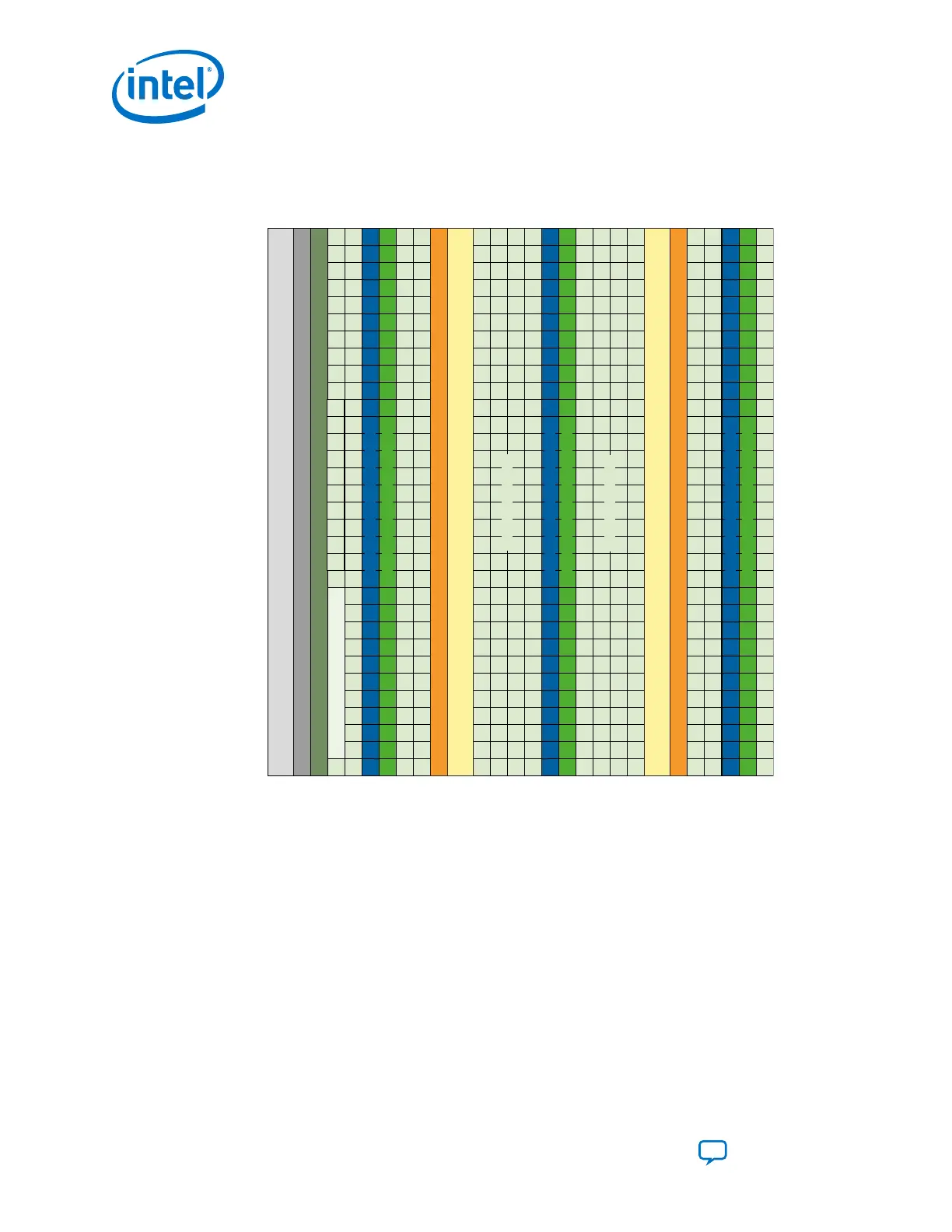
Figure 1. Intel Cyclone 10 GX FPGA Architecture Block Diagram
The transceiver channels are placed on the left side periphery in Intel Cyclone 10 GX devices.
Core Logic Fabric
M20K Internal Memory Blocks
Transceiver Channels
Hard IP Per Transceiver: Standard PCS, Enhanced PCS
PCI Express Gen2 Hard IP
PLLs
M20K Internal Memory Blocks
Variable Precision DSP Blocks
I/O PLLs
Hard Memory Controllers, General-Purpose I/O Cells, LVDS
M20K Internal Memory BlocksM20K Internal Memory Blocks
Variable Precision DSP Blocks
Core Logic Fabric
I/O PLLs
Hard Memory Controllers, General-Purpose I/O Cells, LVDS
M20K Internal Memory BlocksM20K Internal Memory Blocks
Variable Precision DSP Blocks
1.1.1. Intel Cyclone 10 GX Device Transceiver Layout
Intel Cyclone 10 GX devices offer 6-, 10-, or 12-transceiver channel counts. Each
transceiver bank has up to six transceiver channels. Intel Cyclone 10 GX devices also
have one embedded PCI Express Hard IP block.
The figures below illustrate different transceiver bank layouts for Intel Cyclone 10 GX
device variants.
1. Intel
®
Cyclone
®
10 GX Transceiver PHY Overview
UG-20070 | 2018.09.24
Intel
®
Cyclone
®
10 GX Transceiver PHY User Guide
Send Feedback
8