1.1.2. Intel Cyclone 10 GX Device Package Details
The following tables list package sizes, available transceiver channels, and PCI Express
Hard IP blocks for Intel Cyclone 10 GX devices.
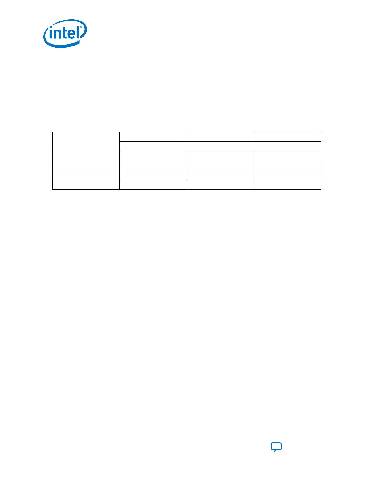
Table 1. Package Details for Devices with Transceivers and Hard IP Blocks Located on
the Left Side Periphery of the Device
• Package U484: 19mm x 19mm package; 484 pins.
• Package F672: 27mm x 27mm package; 672 pins.
• Package F780: 29mm x 29mm package; 780 pins.
Device
U484 F672 F780
Transceiver Count, PCIe Hard IP Block Count
10CX085 6, 1 6, 1 N/A
10CX105 6, 1 10, 1 12, 1
10CX150 6, 1 10, 1 12, 1
10CX220 6, 1 10, 1 12, 1
1.2. Transceiver PHY Architecture Overview
A link is defined as a single entity communication port. A link can have one or more
transceiver channels. A transceiver channel is synonymous with a transceiver lane.
For example, a 10GBASE-R link has one transceiver channel or lane with a data rate of
10.3125 Gbps. A 40GBASE-R link has four transceiver channels. Each transceiver
channel operates at a lane data rate of 10.3125 Gbps. Four transceiver channels give
a total collective link bandwidth of 41.25 Gbps (40 Gbps before and after 64B/66B
Physical Coding Sublayer (PCS) encoding and decoding).
1.2.1. Transceiver Bank Architecture
The transceiver bank is the fundamental unit that contains all the functional blocks
related to the device's high speed serial transceivers.
Each transceiver bank includes four or six transceiver channels in all devices.
The figures below show the transceiver bank architecture with the phase locked loop
(PLL) and clock generation block (CGB) resources available in each bank.
1. Intel
®
Cyclone
®
10 GX Transceiver PHY Overview
UG-20070 | 2018.09.24
Intel
®
Cyclone
®
10 GX Transceiver PHY User Guide
Send Feedback
10