Table of wiring diagrams
1/4
8. Appendix
89000
89000
Table of w iring diagrams
Table of wiring diagrams
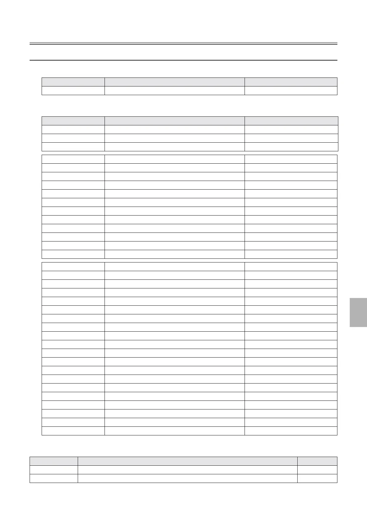
To access the wiring diagrams, click Wiring diagrams in Bookmarks.
!
!!
! Printer section
!
!!
! Processor section
Block No. Item Diagram No.
- System connection diagram J310593
Block No. Item Diagram No.
LP 1-1 AC power supply circuit diagram J310374
LP 1-2 DC power supply circuit diagram (1) J310375
LP 1-3 DC power supply circuit diagram (2) J310376
LP 2-1 AC power supply connecting J310377
LP 2-2 DC power supply connecting J310378
LP 2-3 Around printer control PCB J310380
LP 2-4 Around printer I/O PCB 1 J310381
LP 2-5 Around printer I/O PCB 2 J310382
LP 2-6 Around printer I/O PCB 3 J310383
LP 2-7 Around triple magazine PCB J310384
LP 2-8 Correction value printing unit J310385
LP 2-9 Around laser unit (type HhB) J310386
LP 2-9 Around laser unit (type IiB) J310627
LP 2-10 Around quad magazine PCB J310387
LP 2-11 Around printer I/F PCB J310379
LP 3-1 Frame section SEQ0107
LP 3-2 Magazine mount unit SEQ0108
LP 3-3 Paper supply unit (1) SEQ0109
LP 3-4 Paper supply unit (2) SEQ0110
LP 3-5 Exposure advance unit (1) SEQ0111
LP 3-6 Exposure advance unit (2) SEQ0112
LP 3-7 Paper advance unit 1 SEQ0113
LP 3-8 Paper advance unit 2 (1) SEQ0114
LP 3-9 Paper advance unit 2 (2) SEQ0115
LP 3-10 Paper advance unit 2 (3) SEQ0116
LP 3-11 Laser unit (1) SEQ0117
LP 3-12 Laser unit (2) SEQ0118
LP 3-13 Laser unit (3) (type HhB) SEQ0119
LP 3-13 Laser unit (3) (type IiB) SEQ0201
LP 3-14 Correction value printing unit SEQ0120
LP 3-15 Triple magazine unit SEQ0121
LP 3-16 Quad magazine unit (1) SEQ0122
LP 3-17 Quad magazine unit (2) SEQ0123
LP 3-18 Quad magazine unit (3) SEQ0124
LP 3-19 Quad magazine unit (4) SEQ0125
Block No. Item Diagram No.
PP 1-1 AC power source circuit diagram (outside Japan) (QSS-3701/3702/3703/LP7500/LP7600) J310555
PP 1-1 AC power source circuit diagram (outside Japan) (QSS-3704/3705/LP7700/LP7900) J310554
Distributed by: minilablaser.com