Implementation
Microsemi Proprietary and Confidential UG0677 User Guide Revision 9.0 105
4.5.1 Invoking the Pin Planner
To invoke the Pin Planner, the design must be in the post-synthesis state.
1. Invoke the Constraint Manager from the Design Flow window
(Design Flow > Manage Constraints > Open Manage Constraints View).
2. In the Constraints Manager, select the I/O Attributes tab and then select Edit > Edit with I/O Editor
(I/O Attributes > Edit > Edit with I/O Editor). The I/O Editor opens.
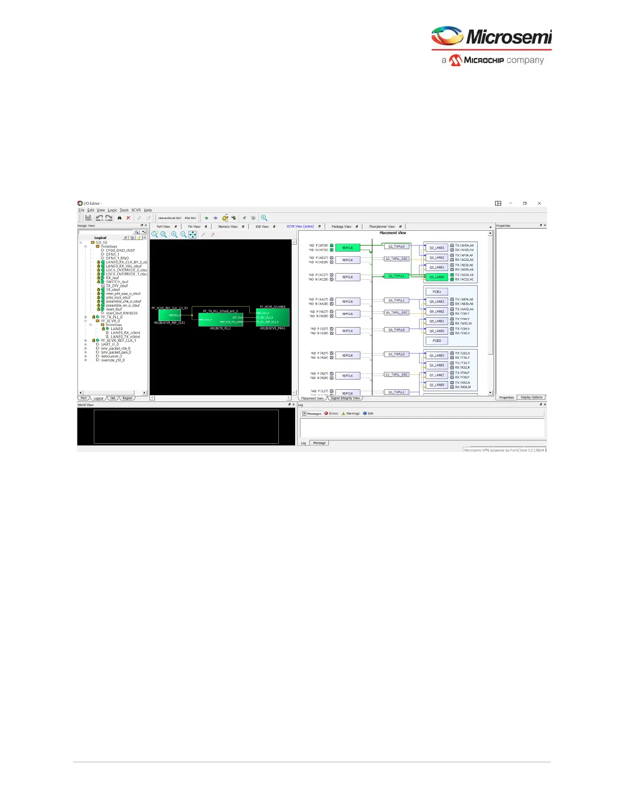
Placement View tab—Presents a physical view of the transceiver connectivity, including transceiver
lanes (XCVR), and Reference Clock (REFCLK), and Transmit PLLs (TxPLL).
Figure 87 • IO Editor GUI
The transceiver view allows you to make assignments—XCVR, REFCLK, and TxPLLs. It has two views:
• A schematic view of the REFCLK, the TXPLL, and the XCVRs they drive.
• A graphical physical view of the REFCLK, its connection from the PADS to the TXPLL and the XCVR
lanes.
The schematic and physical views provide design rule guidance for selecting legal connectivity
combinations between the XCVR I/O, TxPLLs, and REFCLK inputs. It provides logical mapping to the
device physical resources using connection rules of the device.