Functional Description
Microsemi Proprietary and Confidential UG0677 User Guide Revision 9.0 46
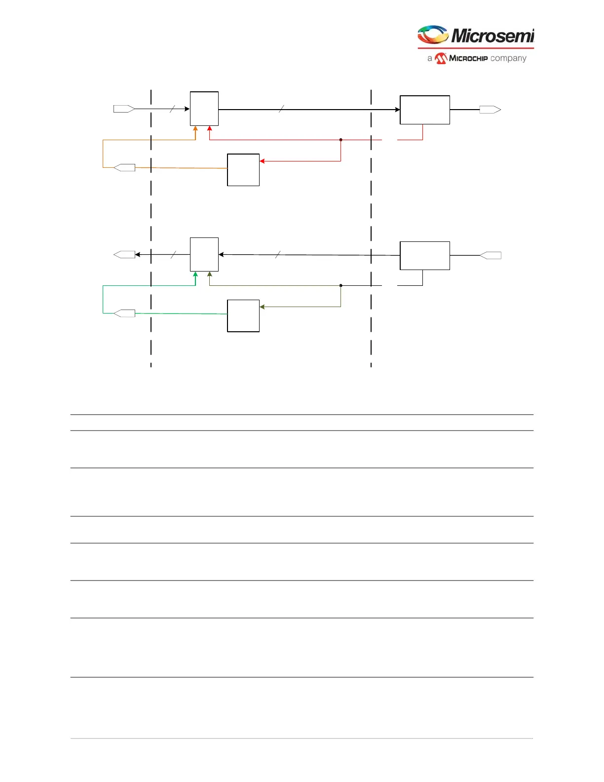
Figure 29 • PMA Only Data Path – Less Than or Equal to 40-bits
The following table lists the port names and description for the PMA mode module.
Table 13 • PMA Port List
Port Name Direction Clock Description
LANE#_CDR_REF_CLK_#/LAN
E#_CDR_REF_CLK_FAB
Input Reference clock to lane CDR. Can be sourced from
either FPGA clock or from a
XCVR_#[A,B,C]REFCLK_P/N pin.
LANE#_CLK_REF Input This port is exposed to user with Half-Duplex option.
LANE#_REF_CLK must be connected by the user
to a stable clock with same clock frequency as
Recovered clock such as the local clock.
LANE#_TX_BIT_CLK_[1:0]
2
Input Clock from BIT_CLK of the XCVR TxPLL. Included
in CLKS_FROM_TXPLL_# BIF (bus interface).
LANE#_TX_PLL_REF_CLK_# Input Input clock from TX_PLL REF_CLK_TO_LANE
output pin. Included in CLKS_FROM_TXPLL_# BIF
(bus interface).
LANE#_TX_PLL_LOCK_# Input Input lock status from TX_PLL LOCK output pin.
Included in CLKS_FROM_TXPLL_# BIF (bus
interface).
LANE#_TX_DATA[N:0]
1
Input TX_CLK_[R:G] Transmits data. The PF_XCVR send/receive order
is low to high byte. The first serial bit appears in bus
bit0. Switching transmission order in PMA mode is
accomplished by reversing the bus connections in
the fabric.
TX
FWF
TX_DATA[N:0]
N= 8, 10,
16, 20,
32, 40
8, 10,
16, 20,
32, 40
Serializer
TXP, TXN
mux
TX_CLK
RX
FWF
RX_DATA[N:0]
N= 8, 10,
16, 20,
32, 40
8, 10,
16, 20,
32, 40
De-Serializer
RXP, RXN
mux
RX_CLK
Clocks appear in
colors. Data path is
black.
div8,
div10,
div16,
div20,
div32,
div40
div8,
div10,
div16,
div20,
div32,
div40
PMA
PCS-PMA Only- Native
FPGA
Fabric