Simulation
Microsemi Proprietary and Confidential UG0677 User Guide Revision 9.0 121
6 Simulation
RTL simulation mode is available for all of the transceiver modes. This simulation mode enables the
simulation of all the protocol communication layers (including the PMA, PCS, and fabric interfaces) and
provides accurate cycle simulation for the design. However, using RTL simulation incurs some run-time
penalties. Microsemi provides a specific PCIe BFM model for enhanced simulation of PCIe designs using
the embedded PCIe controllers, see UG0685: PolarFire FPGA PCI Express User Guide.
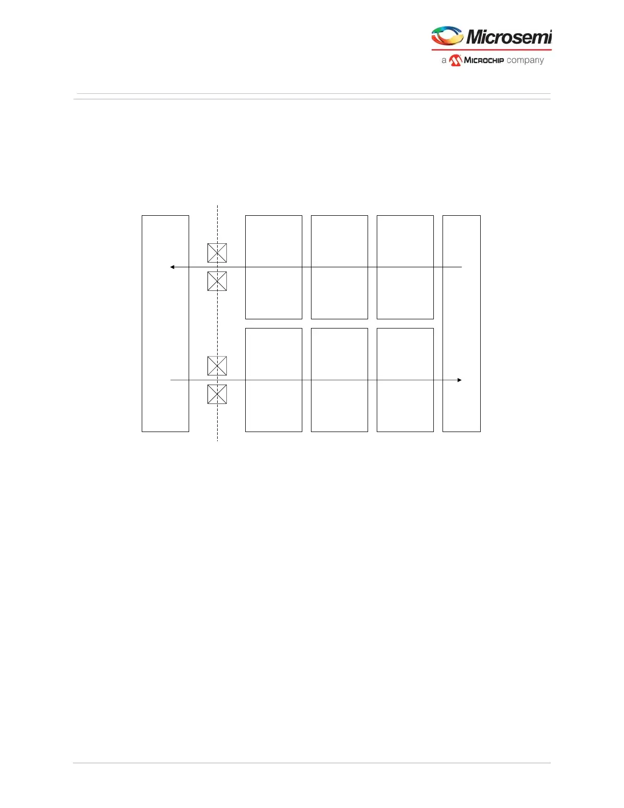
Figure 99 • RTL Simulation Block Diagram
6.1 RTL Simulation Mode
RTL simulation mode simulates the XCVR block from the fabric interface to the serial I/O interface. RTL
simulation mode is available for all of the XCVR modes. This mode supports all of the protocol
communication layers, including the physical layer, and provides accurate cycle simulation for the
design. Using RTL simulation, however, experiences some run-time penalties. As the IP user block is
off-chip, it must be connected to the user design in the top-level test bench. It is the user’s responsibility
to provide the model for the off-chip IP that can communicate with the XCVR block in the same protocol
used by the XCVR block when using this mode.
To minimize simulation time, certain peripherals in the PolarFire transceiver do not have full behavioral
models. These models are replaced with memory models that output a message indicating when the
memory locations inside the peripheral are accessed. The memory models are created by using register
information that is generated by Libero. The XCVR register data is found at <Libero
Project>\component\work\<top_level>\<xcvr_component_name>. The peripheral signals do not toggle
based on any writes to registers, or react to any signal inputs on the protocol pins.
Using RTL simulation mode, the FPGA designer can have an off-chip verification IP model that
communicates with the transceiver. For example, if the design uses a 8b10b XCVR block, the FPGA
designer must have a 8b10b verification IP off-chip block to communicate with the XCVR block using the
required protocol. When the IP user block is off-chip, it must be connected to the design in the top-level
testbench.
User
Verification IP
User FPGA
Design
Transmit PMA
Receive PMA
Transmit PCS
Receive PCS
Transmit Fabric
Interface
Receive Fabric
Interface
XCVR_TXP
XCVR_TXN
XCVR_RXP
XCVR_RXN
Off-Chip