Functional Description
Microsemi Proprietary and Confidential UG0677 User Guide Revision 9.0 69
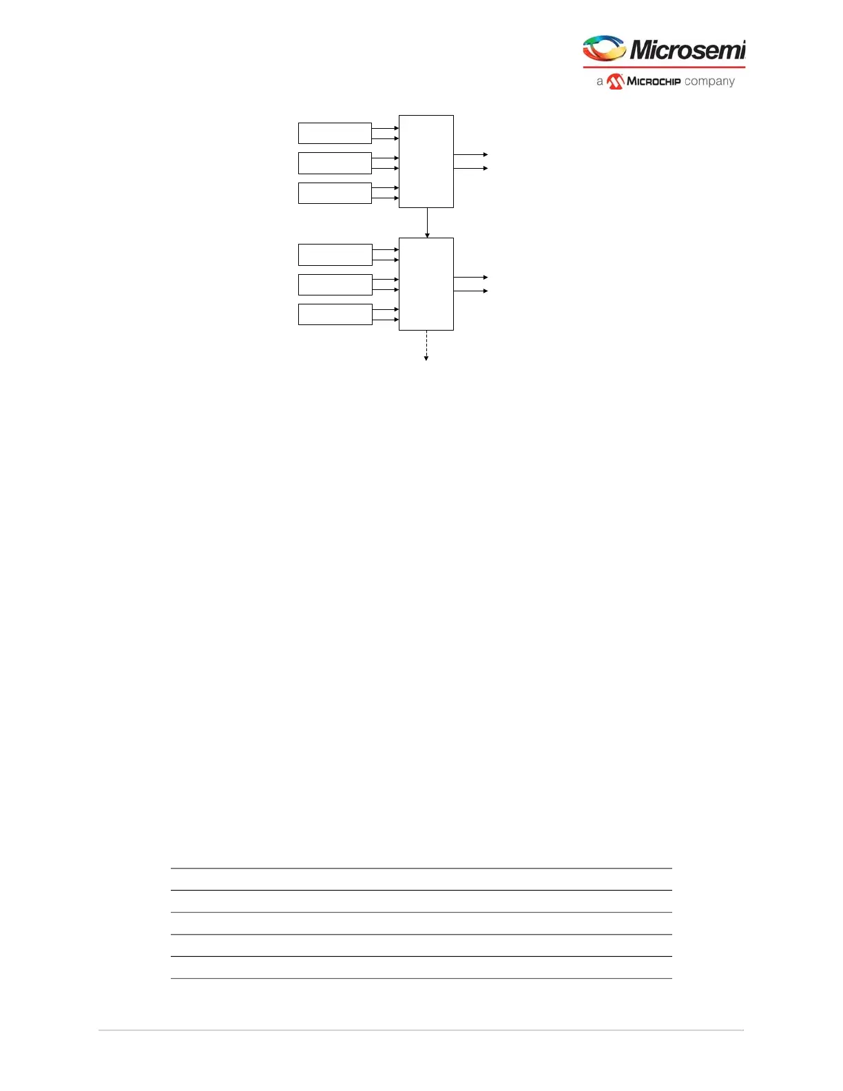
Figure 50 • REFCLK Input Pin Diagram
Note: The XCVR_#[ABC]_REFCLK pins are available per quad. The REFCLK input to the reference clock
interface (see Figure 43, page 62) connects the REFCLK source to the associated TxPLL.
For more information on reference clock interface, see Transceiver Reference Clock Interface, page 61.
3.5.4.4 Reference Clock Disruptions
Reference clocks are required to be applied and stable to the PLLs for proper transceiver operations for
Lock to Data or Lock to Reference applications. TXPLL and RXCDR PLL require a guaranteed reference
clock to ensure proper operation. PolarFire reference clock inputs does not include any "signal
detection". It is the responsibility of the user design to monitor and handle losses or switching of the
system level reference clocks. Reference clock disruptions can cause the lock control circuitry to
misbehave and possibly be stuck into whatever state it is in when the reference clock is lost.
3.5.4.5 Transceiver Resource Layout
For PolarFire devices, there are between one to six transceiver quads with four transceivers each, for a
total of 4 to 24 full-duplex transceiver lanes. There are up to three external reference clock inputs per
quad, which can be used with every transmit PLL and transceiver lane CDRs. See Transceiver Clocks,
page 61 for more information.
The transmit PLL output clocks can be used by one or more lanes within a quad, or shared with adjacent
quads.
Each receive lane CDR has its own PLL; therefore, all receive rates can run at independent frequencies.
For the transmit lanes, one base rate can be created by a transmit PLL and driven to each of the transmit
lanes it can connect to. Each lane can select between the base rate of two different transmit PLLs or a
divided version (Div2, Div4, Div8, or Div11), which can be selected per transmit lane.
The reference clock to the CDR can be sourced from the FPGA fabric thereby allowing more reference
clock sources within a design. The inherent noise from the fabric is tolerated by the CDR.
The following table lists the number of transceiver resources available for each PolarFire family device.
Table 22 • PolarFire Transceiver Resources
Device XCVR Lanes TxPLLs Reference Clock Input Pins
MPF100 8 6 12 single-ended/6 differential
MPF200
1
16 11 22 single-ended/11 differential
MPF300 16 11 22 single-ended/11 differential
MPF500 24 15 30 single-ended/15 differential
XCVR_#A_REFCLK
XCVR_#B_REFCLK
XCVR_#C_REFCLK
Reference
Clock Interface
Block
Reference
Clock Interface
Block
To Local Quad
TXPLLs and CDRs
To Local Quad
TXPLLs and CDRs
To Cascade Clock
XCVR_#A_REFCLK
XCVR_#B_REFCLK
XCVR_#C_REFCLK