Functional Description
Microsemi Proprietary and Confidential UG0677 User Guide Revision 9.0 36
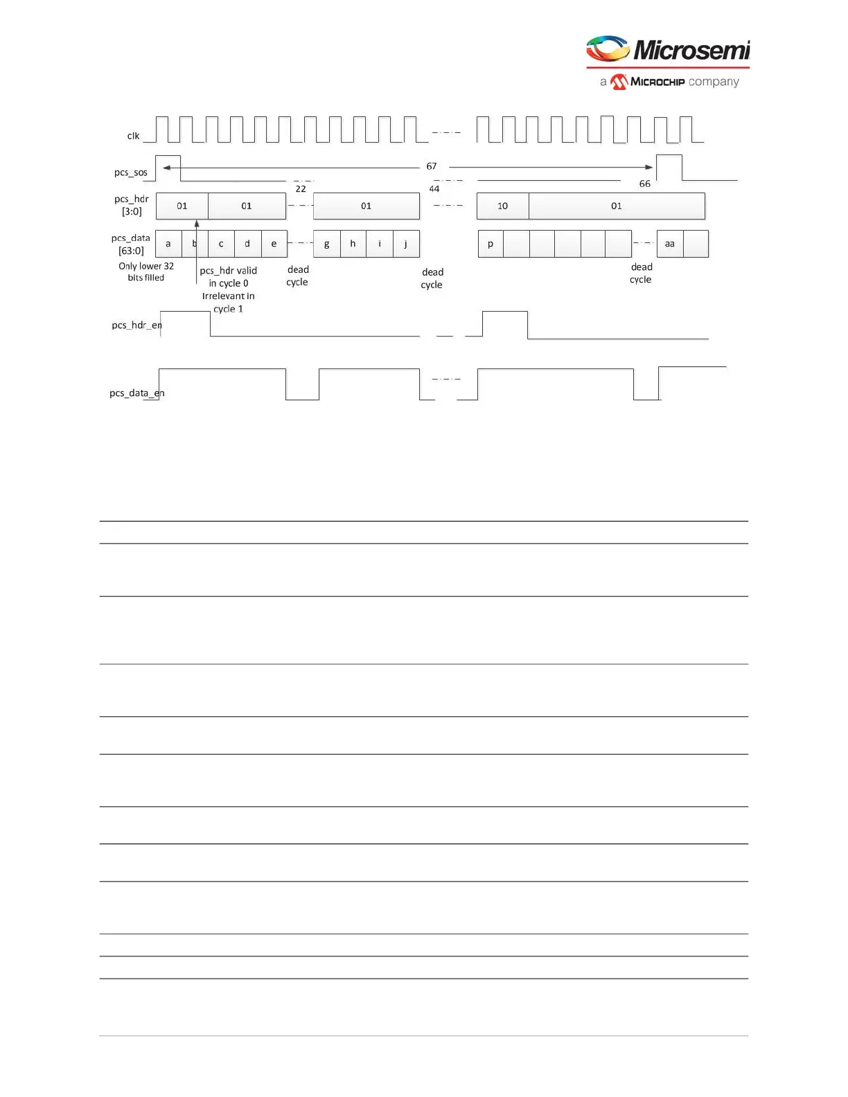
Figure 23 • 64b67b Receive Sequence For 32-Bit Interface
Sequence timing for the 64-bit interface consists of 67 clock beats with dead cycles at beats 22, 44, and
66.
The following table lists the port names and description for the 64b66b/64b67b mode of the PCS module.
See section 49.2.4 of the IEEE 802.3ae specification for more information.
Table 11 • 64b66b/64b67b Port List
Port Name Direction Clock Description
LANE#_CDR_REF_CLK_#/LAN
E#_CDR_REF_CLK_FAB
Input Reference clock to lane CDR. Can be sourced from
either the FPGA clock or from a
XCVR_#[A,B,C]REFCLK_P/N pin.
LANE#_CLK_REF Input This port is exposed to user with Half-Duplex option.
LANE#_REF_CLK must be connected by the user to
a stable clock with same clock frequency as
Recovered clock such as the local clock.
LANE#_TX_PLL_REF_CLK_# Input Input clock from the TX_PLL REF_CLK_TO_LANE
output pin. Included in CLKS_FROM_TXPLL_# BIF
(bus interface).
LANE#_TX_BIT_CLK_0 Input Clock from BIT_CLK of the XCVR TxPLL. Included in
CLKS_FROM_TXPLL_# BIF (bus interface).
LANE#_TX_PLL_LOCK_# Input Input lock status from the TX_PLL LOCK output pin.
Included in CLKS_FROM_TXPLL_# BIF (bus
interface).
LANE#_TX_SOS Input TX_CLK_[R:G] Start-of-sequence pulse for a super frame, the length
of which varies with the mode.
LANE#_TX_HDR[3:0] Input TX_CLK_[R:G] Sync header corresponding to different encoding
types.
LANE#_TX_DATA[63:0] Input TX_CLK_[R:G] Input encoded data from fabric. PF_XCVR
sends/receives bytes in high to low byte order only in
the 64B6xB mode.
LANE#_PCS_ARST_N Input TX_CLK_[R:G] Asynchronous active-low reset for PCS lane.
LANE#_PMA_ARST_N Input TX_CLK_[R:G] Asynchronous active-low reset for the PMA lane.