Implementation
Microsemi Proprietary and Confidential UG0677 User Guide Revision 9.0 88
Note: For information about pin functions, see Table 18, page 62.
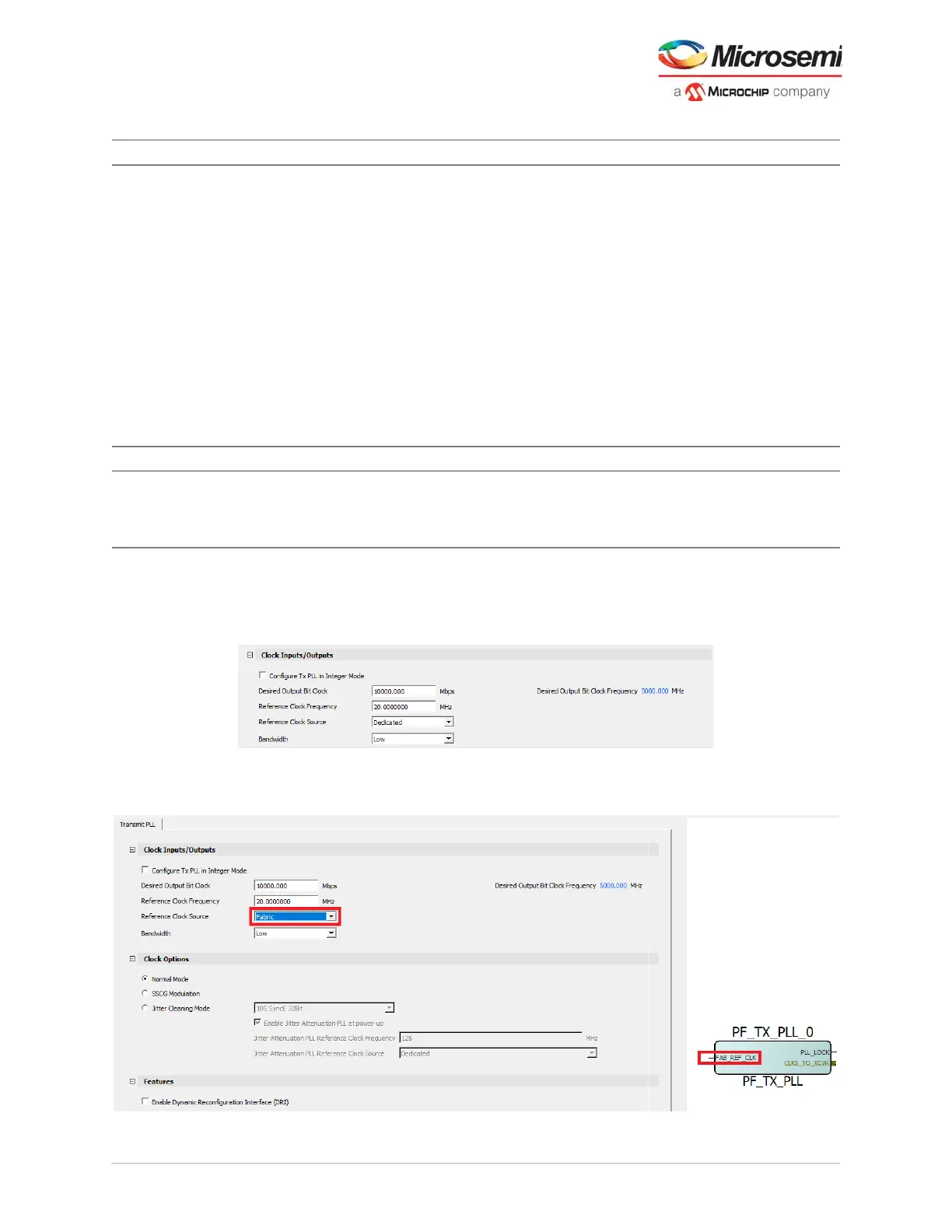
3. Select one of the Reference Clock sources (dedicated source is the default) to define Clock Inputs
and enter the reference clock value.
Figure 65 • Clock Inputs
4. Enter the values in Desired Output Bit Clock. Frequency cannot be entered—it is calculated
automatically based on the speed (data rate in Mbps) and the reference clock.
Figure 66 • Fabric Clock Input
Jitter Cleaning Mode Enable and disable Disabled Radio-button on = disabled
The following options are available when enabled:
10G SyncE 32Bit
10G SyncE 64Bit
1G SyncE 10Bit
CPRI Rate 1
CPRI Rate 2
CPRI Rate 3
CPRI Rate 4
CPRI Rate 5
CPRI Rate 6
CPRI Rate 8 – 64-bit
SDI 3G
SDI HD
SDI SD
Custom Protocol Settings
Features
Enable Dynamic
Reconfiguration
Interface (DRI)
Enable and disable Disabled Adds Pins to TXPLL component for using Dynamic
Reconfiguration Interface. See UG0725: PolarFire
FPGA Device Power-Up and Resets User Guide for
DRI information.
Table 27 • Transmit PLL Configurator GUI Options
Clock Inputs Options Default Details