Functional Description
Microsemi Proprietary and Confidential UG0677 User Guide Revision 9.0 66
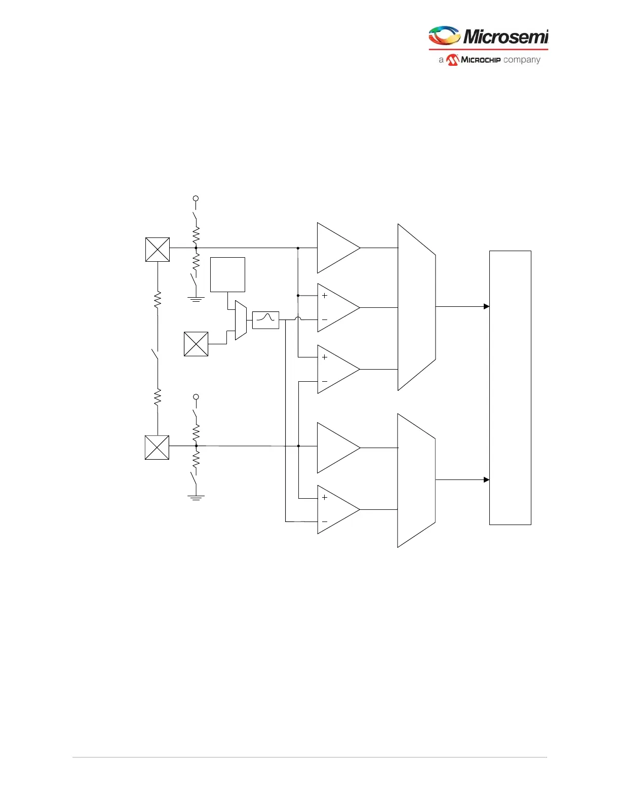
3.5.4.3 Dedicated Reference Clock Input Pins
For every transmit PLL within the transceiver PMA, there is a reference input pin pair for an external input
of reference clocks to the device, as shown in the following figure. The reference clock inputs provide
flexibility to interface with both single-ended and differential clocks and can drive up to two independent
clocks per transceiver quad. The reference clock inputs has a single power supply (VDD_XCVR_CLK)
that is shared across all reference clock buffers. These reference clocks can also be sourced for the
global and regional clock networks in the FPGA fabric of the PolarFire devices.
The following figure provides a detailed view of the dedicated reference clock.
Figure 49 • Dedicated Transceiver Reference Clock Inputs
Note: For more information on reference clock interface block, see Figure 43, page 62.
3.5.4.3.1 Differential Input
This mode supports differential inputs such as LVDS/HCSL. The differential reference clock is available
on REFCLK0 (REFCLK1 is not available with differential input clock mode). The inputs include an
optional on-die 100 differential termination resistor. By default, the differential input termination
resistance is set in high-Z mode until programmed with Libero software. XCVR_VREF is not used for
differential reference clock input signaling. XCVR_VREF is used for single-ended signals requiring a
voltage reference such as SSTL.
CMOS
CMOS
REF
DIFF
REF
Termination
Termination
XCVR_VREF
XCVR_REFCLK_P
XCVR_REFCLK_N
REFCLK
Interfac
e Block
REFCLK0
REFCLK1
VDD_XCVR_CLK
VDD_XCVR_CLK
Filter
Internal
Reference
Voltage
Circuit
Differential
Termination