Functional Description
Microsemi Proprietary and Confidential UG0677 User Guide Revision 9.0 62
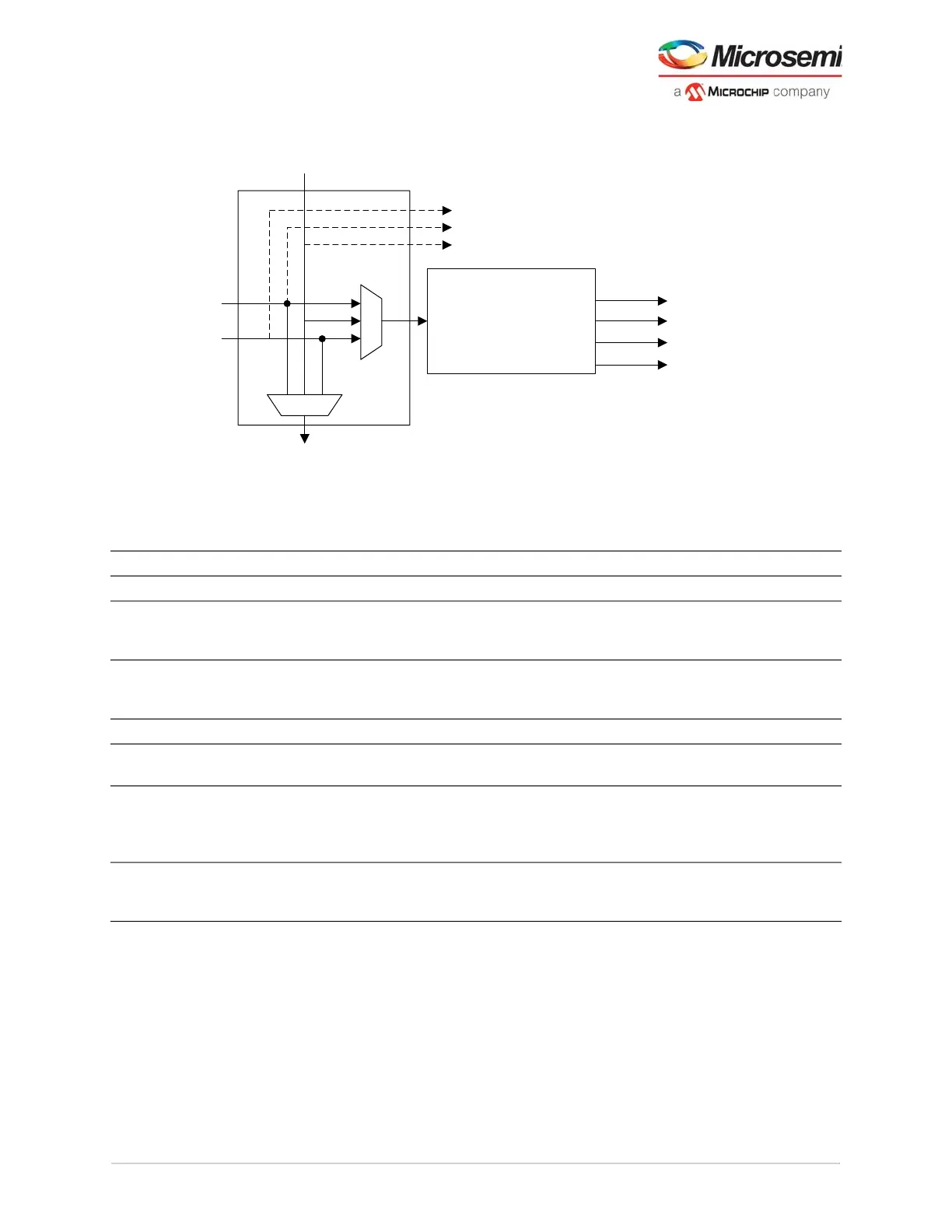
Figure 43 • Reference Clock (REFCLK) Interface to Transmit PLL
The following table lists the transmit PLL pins.
There are some use-cases which can allow a XCVR quad's global output to be used to broadcast the
SerDes REFCLK, if that XCVR is configured to use regional clocks for the TX/RX clocks allowing these
specific use-cases to broadcast the SerDes REFCLK into the FPGA fabric with a more predictable
amount of clock jitter.
Table 18 • Transmit PLL Pin List
1
1. Pin list for both Q#_TxPLL[1:0] and Q#_TxPLL_SSC PLLs.
Name Direction Description
REF_CLK Input Transmit PLL input clock from reference clock interface (Figure 43, page 62).
PLL_LOCK Output PLL_LOCK is the PLL lock indicator signal that can be used to drive logic in the
fabric. It is a fabric routed signal.
(High = LOCK).
CLKS_TO_XCVR Output CLKS_TO_XCVR is a bus interface port (BIF) with three outputs that are
required to be interconnected between the TXPLL and the XCVR components.
The BIF includes BIT_CLK, LOCK, and REF_CLK_TO_LANE outputs.
BIT_CLK
2
2. Port is a part of the bus interface port (BIF) CLKS_TO_XCVR.
Output High-speed clock to lane.
LOCK
2
Output Connected to the TX_PLL_LOCK_0/1 input port, which is a part of the
CLKS_FROM_TXPLL_0/1 BIF on the XCVR block. It is a hardwired connection.
REF_CLK_TO_LANE
2
Output Connected to the TX_PLL_REF_CLK_0/1 input port, which is a part of the
CLKS_FROM_TXPLL_0/1 BIF on the XCVR block. It is a hardwired connection.
TXPLL reference clock that is passed to the XCVR lane clock (used for
simulation only)
CLK_125 Output Exposed directly on the TXPLL block. Its frequency is fixed at
125 MHz. It is exposed only when the TXPLL BIT_CLK is
2500 Mbps, and must be used for a PCIe use case.
REFCLK0
CLKS_TO_XCVR[BIF]
REFCLK1
Cascade from
Upper REFCLK
Cascade to
Lower
REF_CLK
REF_CLK_TO_LANE
TXPLL
REFCLK
Interface
TXPLL= TXPLL_SSC or
TXPLL0 or TXPLL1
To Local Quad
CDRs
LOCK
BIT_CLK
PLL_LOCK