Functional Description
Microsemi Proprietary and Confidential UG0677 User Guide Revision 9.0 55
3.5 Transceiver Clocking
Clocking of PolarFire transceivers uses several dedicated resources that are embedded in each device.
All XCVR designs require a XCVR_REF_CLK to provide and clock input to a XCVR_TXPLL, which
provides the necessary clocks for the XCVR_LANE or XCVR_LANES. The XCVR_TXPLL synthesizes
the input reference clock to generate the high-speed serial clock used in the transmitter PMA.
XCVR_REF_CLKs and XCVR_TXPLLs are shared and used for several high-speed serial protocols.
3.5.1 Transmit PLL
Two variations of the transmit PLLs embedded within the transceiver lanes are available based on
protocol requirements. Both TxPLLs use ring VCO-based PLLs. Using a combination of TxPLL ranges
and post-dividers produce frequencies across the entire supported range of the device. The transmit
PLLs include one type with spread-spectrum (SSCG) generation modulation capabilities (TXPLL_SSC)
and another type without SSCG capabilities (TxPLL). Both types of transmit PLLs use the same half-rate,
fractional-N type (Frac-N) architecture design, thereby relaxing the speed requirements of the phase
detector and frequency dividers. This consequently expands the VCO tuning range and enhances the
phase noise performance while having a significant impact on the total power. The transmit PLL phase
detector provides a valid output while driving a full-rate random data stream on both edges using the half-
rate clock. All transmit PLLs support a jitter-attenuator option. The jitter attenuator is used to track the
data rate of any noisy reference clock with a clean input reference clock to provide a 0 ppm offset from
the noisy reference clock while providing a jitter-cleaned output.
Each transceiver lane can select a transmit clock from the transmit PLLs that are close enough to drive
their half rate clock (Figure 38, page 55). The PLL uses the input reference clock to generate a serial bit
clock (at half the rate). The transmit PLL detects and signals a loss of lock in the event that the reference
clock stops toggling or when the reference clock transitions to an incorrect frequency.
There are also instances that include additional transmit PLLs, which can be used by the local
transceiver quad and in a subset of lanes of adjacent quads.
The output frequency of each transmit PLL is derived automatically from the reference clock frequency
and the settings for the PLL multipliers. Each transmit lane can then divide this base transmit PLL rate
per lane using the post-divider by 1, 2, 4, 8, or 11. The resulting frequency is half the bit rate based on the
transmit half-rate architecture. For example, a 2.5 GHz clock is used for a 5 Gbps transmit transceiver
line rate. The programmable multipliers are defined and programmed by the Libero transceiver interface
configurator as per the desired protocol.
In addition, the transmit PLL can also provide the system clock for the FPGA logic.
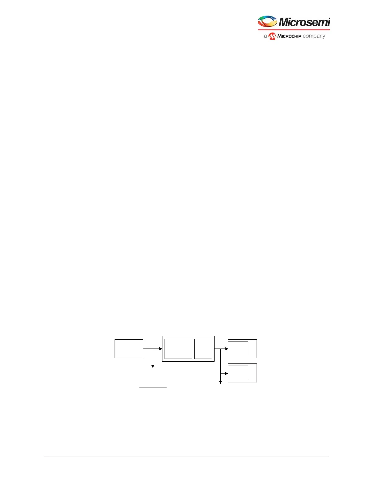
Figure 38 • Transmit PLL
Two different types of transmit PLLs can be used with the transceiver based on half-rate architecture.
Both PLL types have identical analog portions with only digital logic differences, therefore each PLL type
has identical performance.
3. Typically, these interfaces are implemented uni-directional. For full duplex, the RX interface and TX interface clock can not be
global or global (Shared) at the same time as only one global clock is supported per transceiver quad. If using the RX and TX both
as global is required by design, the design must use two separate XCVR configurations (instances), one in RX half duplex mode
and other in TX half duplex mode.
Transmit PLL
Reference
Clock
Network
Rx CDR
Tx
Divider
Jitter
Attenuation
/Spread
Spectrum
Frac-N
Lane Tx
Tx
Divider
Lane Tx