Implementation
Microsemi Proprietary and Confidential UG0677 User Guide Revision 9.0 84
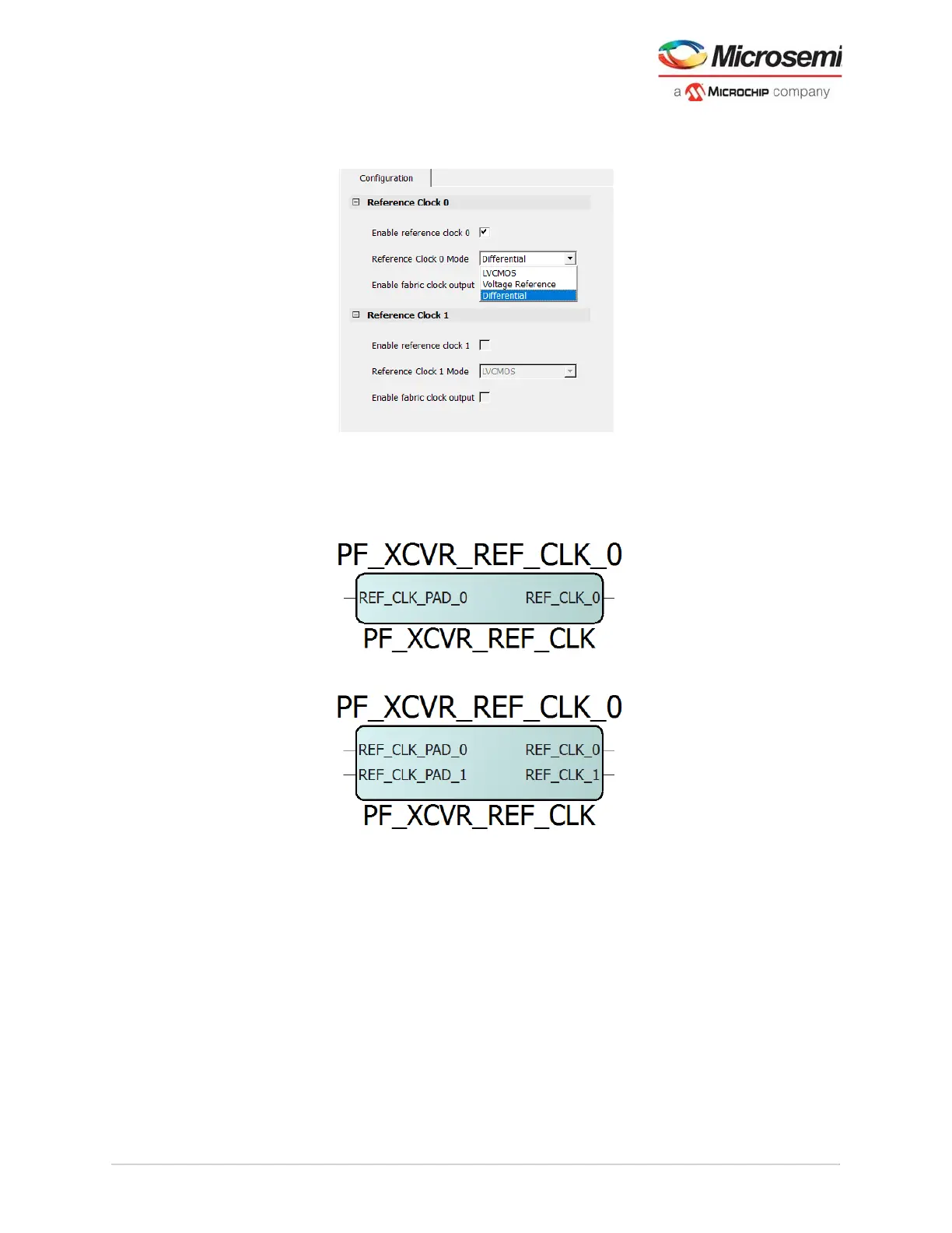
3. Select the reference clock mode type based on the input buffer type in the application.
Single-ended Differential is the default mode.
Figure 58 • Transceiver Reference Clock Mode Type
In the case of LVCMOS or Voltage Reference inputs, the design can have up to two individual reference
clock inputs in one instance of the PF_XCVR_REF_CLK. This configuration can access either or both
Reference Clock 0 or/and 1.
Figure 59 • PF_XCVR_REF_CLK With One Single-Ended Input and Single Output Clock
Figure 60 • PF_XCVR_REF_CLK With Two Single-Ended Input and Two Output Clock
However, only one reference clock input is available when the designer selects Differential (Figure 58,
page 84). In this case, only Reference Clock 0 can be accessed and use a differential clock source
signal.