Functional Description
Microsemi Proprietary and Confidential UG0677 User Guide Revision 9.0 50
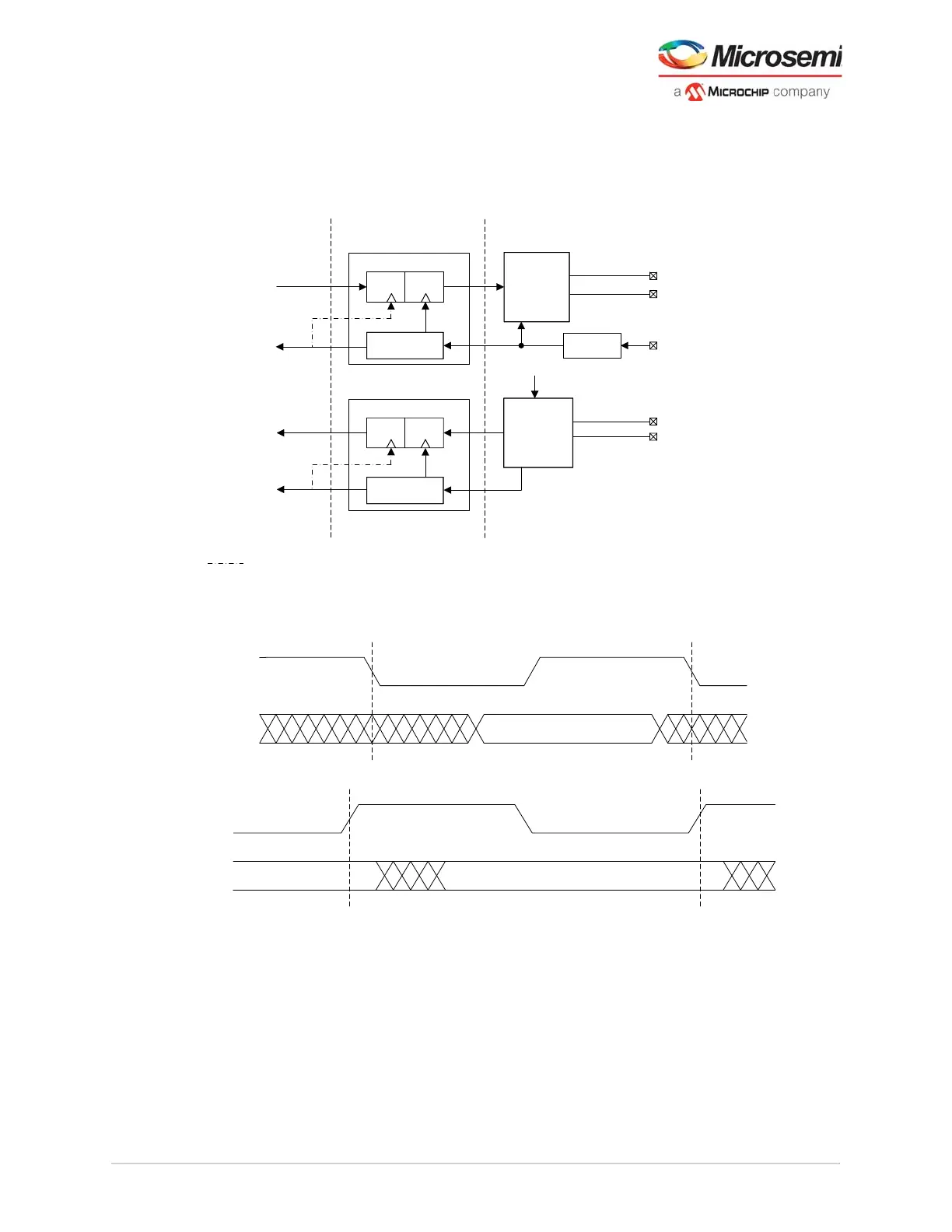
In the transmit direction, data from the fabric or PCS is passed through the FWF with a clock from the
FWF ensuring synchronous clock and data relationships passing to the PMA interface. The FWF is
optionally selected in the Libero Transceiver Configurator by choosing the correct global or regional
interface clock option, see Table 32, page 94.
Figure 31 • Non-Deterministic Interface With FWF
The FWF provides clock domain crossing functionality to manage clock and data setup and hold. The
following figures show the timing relationships of transmit and receive data paths at the fabric interface.
Figure 32 • Non-Deterministic Interface Transmit Timing Waveform
Figure 33 • Non-Deterministic Transceiver Receive Timing Waveform
Transmit
PMA
Regional or
Global Clocks
XCVR_TX
TXPLL
XCVR_REFCLK
TX_DATA
Receive
PMA
RX_DATA
Recovered Clock
REFCLK
XCVR_RX
PCS/FPGA Fabric
TX_CLK_OUT
RX_CLK_OUT
Regional or
Global Clocks
Phase
Compensator
Phase
Compensator
Fly-wheel FIFO
Fly-wheel FIFO
Tx and Rx PCS to FPGA
Fabric Interface
This connection only visible within the Libero generated component.