Debug and Testing
Microsemi Proprietary and Confidential UG0677 User Guide Revision 9.0 123
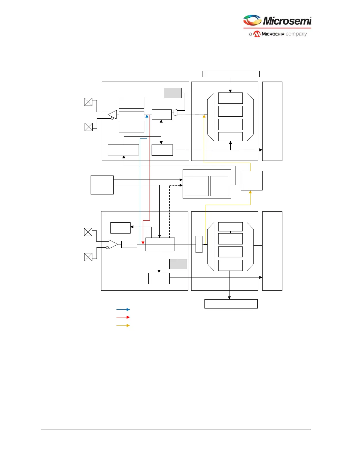
This loopback is after the CDR which requires the receive and transmit paths to have exactly matched
clock rates or 0 ppm differences. In the Far-end loopback case, the LANE#_RX_READY must be used
instead of LANE#_RX_VAL to indicate valid data path.
Figure 100 • Transceiver Loopbacks
Transmit
PCS/
Fabric
Interface
Transmit
PMA
PCIe Sub-System (PCIESS)
Transmit
PCS
Receive
PMA
Transmit PLL
Reference
Clock
Network
Receive
PCS
Polarity
Receive
PCS/
Fabric
Interface
PCIe Sub-System (PCIESS)
8b10b
Encoder
64b/6xb
Encoder
PCIe/PIPE
Pre-/Post-
Emphasis
Serializer
PCS
Divider
Out of Band
Electrical
Idle
PMA Only
CTLE
Eye
Monitor
Jitter
Attenuation
or Spread
Spectrum
Frac-N
PLL
8b10b
Decoder
64b/6xb
Decoder
PCIe/PIPE
PMA Only
PCS
Divider
÷ 1, 2, 4, 8, 11
CDR w/DFE
Deserializer
Loopback
FIFO
XCVR_TXP
XCVR_TXN
XCVR_RXP
XCVR_RXN
CTLE: Continuous Time Linear Equalization
EQ Far-End Loopback
EQ Near-End Loopback
CDR Far-End Loopback
Optional path used
with Jitter
Attenuation
PRBS
Gen
PRBS
Chk