Functional Description
Microsemi Proprietary and Confidential UG0677 User Guide Revision 9.0 8
Figure 2 • Transceiver Receiver
3.1.1.1 Receive Input Buffer
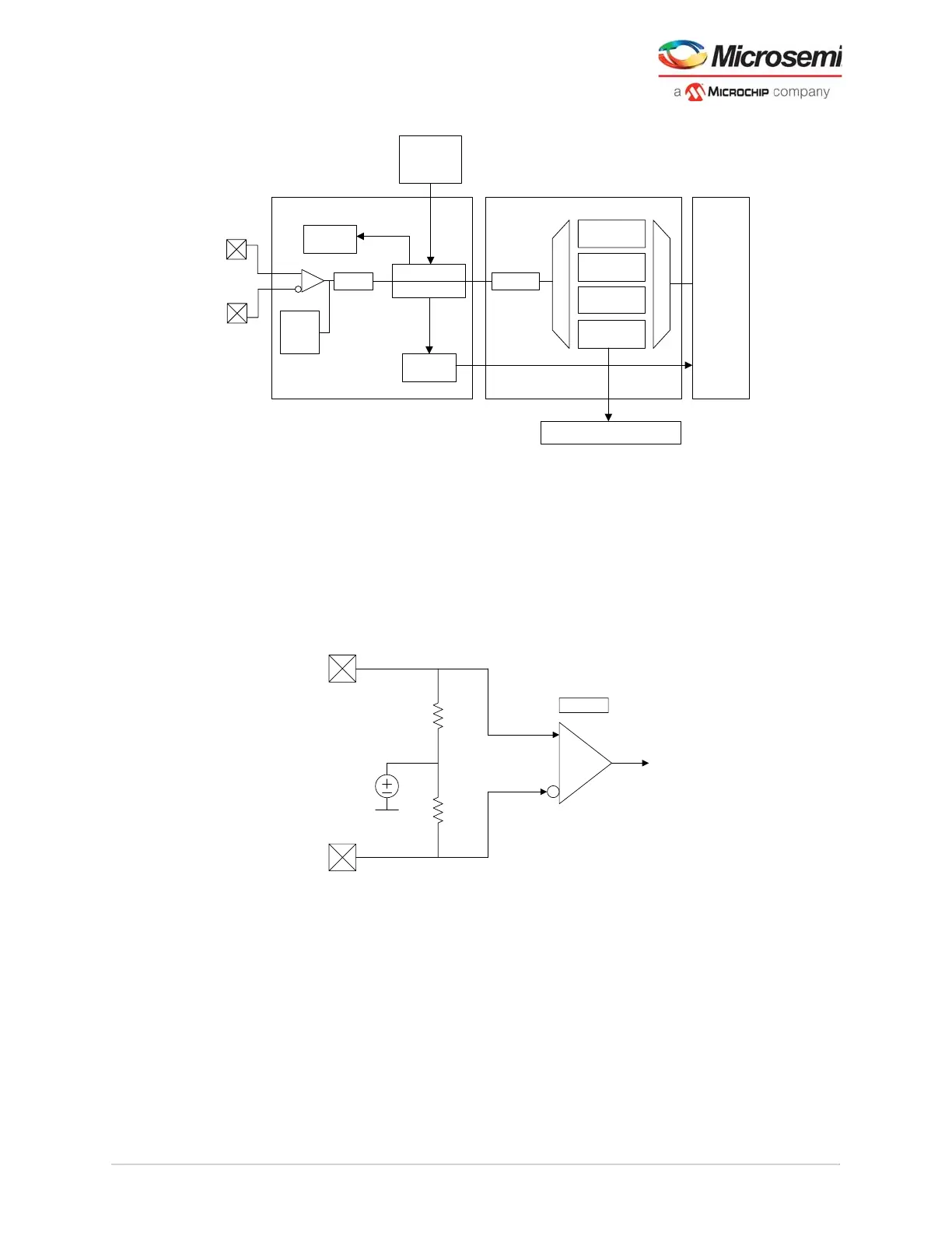
The receiver provides an external input interface through differential pins, XCVR_RXP/N, as shown in
the following figure. The receiver includes a current mode logic (CML) input buffer with programmable
DC restoration that is used in either AC- or DC-coupled applications.
The receive buffer provides an on-die differential termination scheme which can be programmed to 85 ,
100 , or 150 . The receiver buffer also includes a high-impedance (high-Z) mode for hot-swap
capability when the device is powered off. Additionally, the receiver input supports logical swapping of the
polarity of the P and N pins for added flexibility.
Figure 3 • Receiver Input Buffer
Note: VICM is connected to VDDA when AC-coupled link is configured. DC-coupled configurations effectively
disconnects VICM source. See AC/DC Coupled Connection, page 110.
Each receiver lane includes optional signal threshold detection circuitry that users can select according
to protocol or application requirements. This feature identifies whether the signal level present at the
receiver input buffer is above the signal detect threshold voltage needed to trip or activate the receiver
input, which prevents false activity on the receiver path. The signal detection has both a high and low
signal detector. The Libero SoC software configurator provides the correct setting based on protocol or
customization.
Note: The user can also use a JTAG-based interface from SmartDebug to experiment with receiver settings.
Receive PMA Receive PCS
Polarity
Receive
PCS/
Fabric
Interface
PCIe Sub-System (PCIESS)
CTLE
Eye
Monitor
8b10b
Decoder
64b/6xb
Decoder
PCIe/PIPE
PMA Only
PCS
Divider
CDR w/DFE
Deserializer
Reference
Clock
Network
XCVR_RXP
XCVR_RXN
Signal
Detect
CTLE
VICM
Input Common-Mode
Voltage
XCVR_RXP
XCVR_RXN
On-Die Termination
LOS Detect