Functional Description
Microsemi Proprietary and Confidential UG0677 User Guide Revision 9.0 52
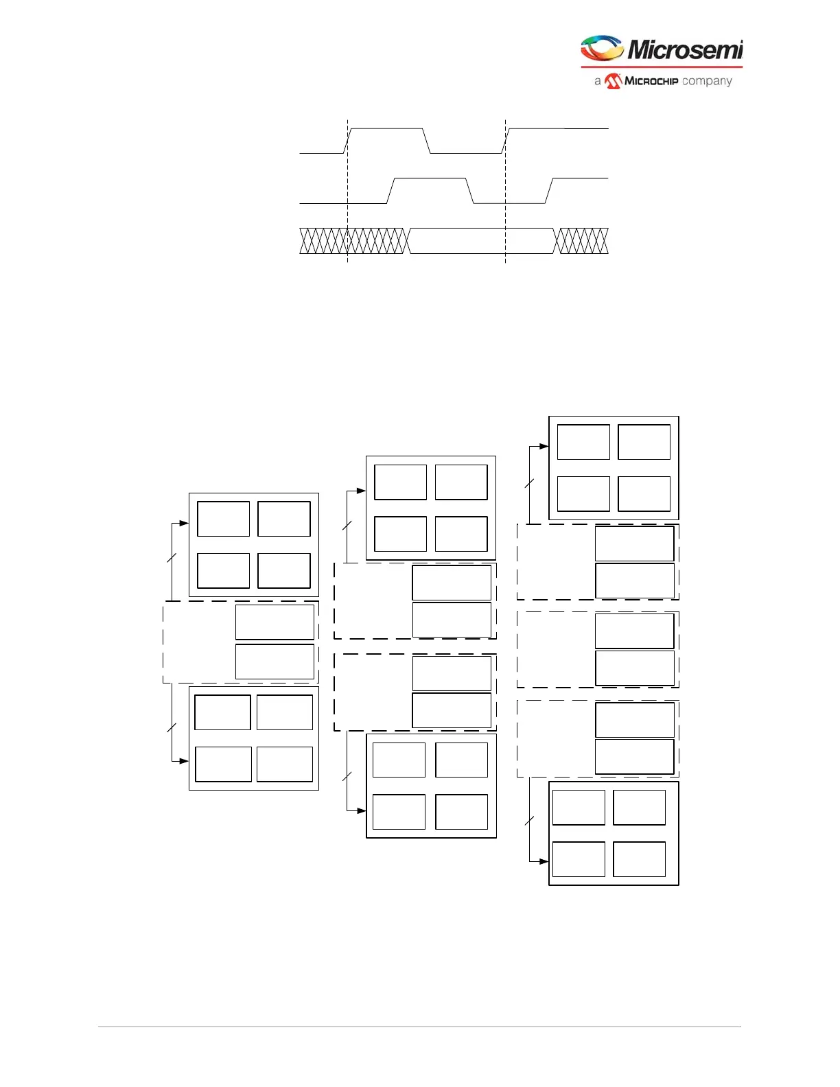
Figure 36 • Deterministic Transceiver Receive Timing Waveform
3.4.3 Transceiver Clock Regions
Two regional clock buffers per transceiver lane (eight per transceiver quad) come from the transceiver.
These interconnections are the basis for specific regions that the particular Quads can drive. These
regions vary from device to device within the family. These regions have a predetermined connectivity to
fabric resources, CCC, and IOs.
Figure 37 • Transceiver Clock Regions
RX_CLK
RX_CLK
(at fabric FF)
RXDATA Valid
Note: RXCLK_FABRIC at PCS I/F after Regional clock route
QUAD0
PLL0_NE PLL1_NE
DLL0_NE DLL1_NE
CCC_NE
PLL0_SE PLL1_SE
DLL0_SE DLL1_SE
CCC_SE
QUAD1
2
2
MPF100T
QUAD0
PLL0_NE PLL1_NE
DLL0_NE DLL1_NE
CCC_NE
PLL0_SE PLL1_SE
DLL0_SE DLL1_SE
CCC_SE
QUAD1
QUAD2
QUAD3
2
2
MPF200T and MPF300T
QUAD1
PLL0_NE PLL1_NE
DLL0_NE DLL1_NE
CCC_NE
PLL0_SE PLL1_SE
DLL0_SE DLL1_SE
CCC_SE
QUAD3
QUAD0
QUAD5
QUAD2
QUAD4
2
2
MPF500T
Regions are depicted by dashed boundary
One Region
Top Region
Top Region
Bottom
Region
Bottom
Region
Middle
Region