2 Design
2 - 16
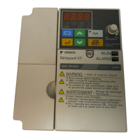
High-function General-purpose Inverter 3G3RX-V1 User’s Manual (I578-E1)
The table below shows the arrangement of the control circuit terminal block, and description and
specifications of each terminal.
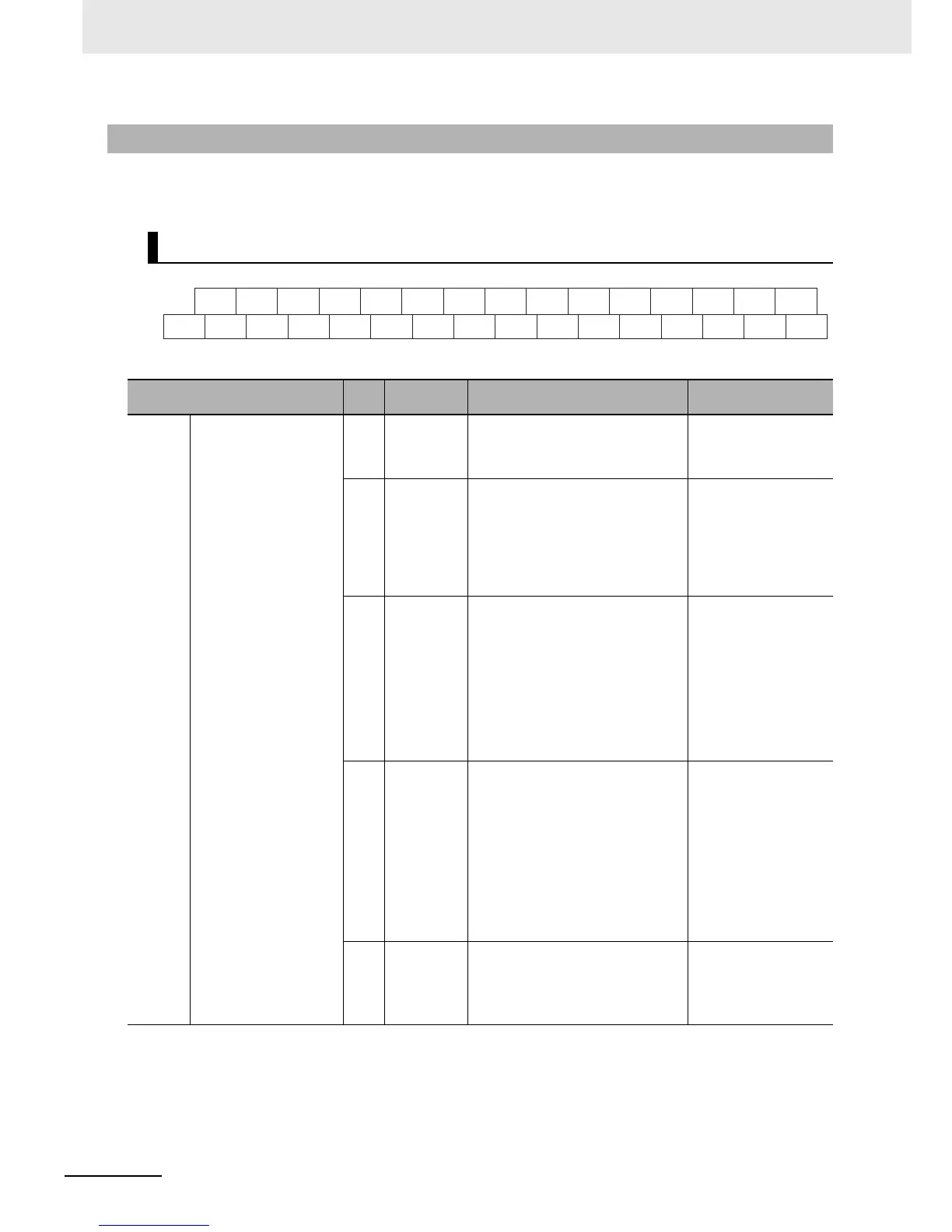
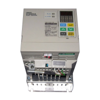
2-3-3 Arrangement and Function of Control Circuit Terminal Block
Control Circuit Terminal Block
Terminal
Terminal
symbol
Terminal
name
Description Specifications
Analog Frequency reference input
FS
Frequency
reference
power supply
output
+10 VDC power supply for the terminal
FV.
Allowable load current:
20 mA max.
FV
Frequency
reference
input (Voltage
reference)
0 to 10 VDC analog input.
By default, this is set so that the
frequency reaches the maximum at 9.8
V (Adjustable in A012/A014).
This terminal is enabled when
Frequency Reference Selection (A001)
is set to 01 (Terminal).
Input impedance: 10 kΩ
Allowable input voltage
range: –0.3 to 12 VDC
FE
Auxiliary
frequency
reference
input (Voltage
reference)
–10 to 10 VDC analog input.
By default, this is set so that the
frequency reaches the maximum at 9.8
V (Adjustable in A112/A114).
Setting these parameters adds the
terminal FE signal to the frequency
reference signal at the terminal FV or FI.
It is also possible to input the frequency
reference independently to the terminal
FE.
Input impedance: 10 kΩ
Allowable input voltage
range: 0 to ±12 VDC
FI
Frequency
reference
input (Current
reference)
4 to 20 mA analog DC input.
By default, this is set so that the
frequency reaches the maximum at
19.8 mA (Adjustable in A102/A104).
By default, the terminal FI signal is
added to the frequency reference signal
at the terminal FV.
If any of the multi-function input
terminals is set to AT, this terminal is
enabled only when the AT terminal is
ON.
Input impedance: 100 Ω
Max. allowable current:
24 mA
FC
Frequency
reference
common
Common terminal for the frequency
setting signals (FV, FE and FI) and the
analog output terminals (AM and AMI).
Do not connect this terminal to the
ground.
–